Chemical vapor deposition (CVD) is a vacuum deposition method used to produce high-quality, and high-performance, solid materials. The process is often used in the semiconductor industry to produce thin films.
A semiconductor is a material which has an electrical conductivity value falling between that of a conductor, such as copper, and an insulator, such as glass. Its resistivity falls as its temperature rises; metals behave in the opposite way. Its conducting properties may be altered in useful ways by introducing impurities ("doping") into the crystal structure. When two differently doped regions exist in the same crystal, a semiconductor junction is created. The behavior of charge carriers, which include electrons, ions, and electron holes, at these junctions is the basis of diodes, transistors, and most modern electronics. Some examples of semiconductors are silicon, germanium, gallium arsenide, and elements near the so-called "metalloid staircase" on the periodic table. After silicon, gallium arsenide is the second-most common semiconductor and is used in laser diodes, solar cells, microwave-frequency integrated circuits, and others. Silicon is a critical element for fabricating most electronic circuits.
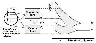
In solid-state physics and solid-state chemistry, a band gap, also called a bandgap or energy gap, is an energy range in a solid where no electronic states exist. In graphs of the electronic band structure of solids, the band gap refers to the energy difference between the top of the valence band and the bottom of the conduction band in insulators and semiconductors. It is the energy required to promote an electron from the valence band to the conduction band. The resulting conduction-band electron are free to move within the crystal lattice and serve as charge carriers to conduct electric current. It is closely related to the HOMO/LUMO gap in chemistry. If the valence band is completely full and the conduction band is completely empty, then electrons cannot move within the solid because there are no available states. If the electrons are not free to move within the crystal lattice, then there is no generated current due to no net charge carrier mobility. However, if some electrons transfer from the valence band to the conduction band, then current can flow. Therefore, the band gap is a major factor determining the electrical conductivity of a solid. Substances having large band gaps are generally insulators, those with small band gaps are semiconductor, and conductors either have very small band gaps or none, because the valence and conduction bands overlap to form a continuous band.

Silicon carbide (SiC), also known as carborundum, is a hard chemical compound containing silicon and carbon. A semiconductor, it occurs in nature as the extremely rare mineral moissanite, but has been mass-produced as a powder and crystal since 1893 for use as an abrasive. Grains of silicon carbide can be bonded together by sintering to form very hard ceramics that are widely used in applications requiring high endurance, such as car brakes, car clutches and ceramic plates in bulletproof vests. Large single crystals of silicon carbide can be grown by the Lely method and they can be cut into gems known as synthetic moissanite.
Wide-bandgap semiconductors are semiconductor materials which have a larger band gap than conventional semiconductors. Conventional semiconductors like silicon have a bandgap in the range of 0.6 – 1.5 electronvolt (eV), whereas wide-bandgap materials have bandgaps in the range above 2 eV. Generally, wide-bandgap semiconductors have electronic properties which fall in between those of conventional semiconductors and insulators.
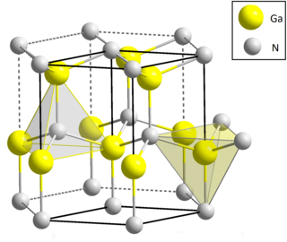
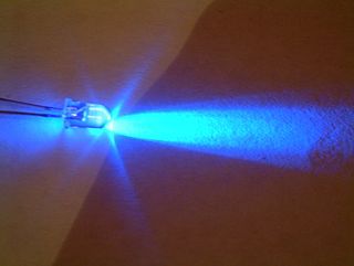
Gallium nitride is a binary III/V direct bandgap semiconductor commonly used in blue light-emitting diodes since the 1990s. The compound is a very hard material that has a Wurtzite crystal structure. Its wide band gap of 3.4 eV affords it special properties for applications in optoelectronic, high-power and high-frequency devices. For example, GaN is the substrate which makes violet (405 nm) laser diodes possible, without requiring nonlinear optical frequency-doubling.
Aluminium nitride (AlN) is a solid nitride of aluminium. It has a high thermal conductivity of up to 321 W/(m·K) and is an electrical insulator. Its wurtzite phase (w-AlN) has a band gap of ~6 eV at room temperature and has a potential application in optoelectronics operating at deep ultraviolet frequencies.

In chemistry, a dangling bond is an unsatisfied valence on an immobilized atom. An atom with a dangling bond is also referred to as an immobilized free radical or an immobilized radical, a reference to its structural and chemical similarity to a free radical.
In chemistry, a nitride is an inorganic compound of nitrogen. The "nitride" anion, N3- ion, is very elusive but compounds of nitride are numerous, although rarely naturally occurring. Some nitrides have a found applications, such as wear-resistant coatings (e.g., titanium nitride, TiN), hard ceramic materials (e.g., silicon nitride, Si3N4), and semiconductors (e.g., gallium nitride, GaN). The development of GaN-based light emitting diodes was recognized by the 2014 Nobel Prize in Physics. Metal nitrido complexes are also common.
Indium gallium arsenide (InGaAs) is a ternary alloy of indium arsenide (InAs) and gallium arsenide (GaAs). Indium and gallium are group III elements of the periodic table while arsenic is a group V element. Alloys made of these chemical groups are referred to as "III-V" compounds. InGaAs has properties intermediate between those of GaAs and InAs. InGaAs is a room-temperature semiconductor with applications in electronics and photonics.
Thermophotovoltaic (TPV) energy conversion is a direct conversion process from heat to electricity via photons. A basic thermophotovoltaic system consists of a hot object emitting thermal radiation and a photovoltaic cell similar to a solar cell but tuned to the spectrum being admitted from the hot object.
Indium gallium nitride is a semiconductor material made of a mix of gallium nitride (GaN) and indium nitride (InN). It is a ternary group III/group V direct bandgap semiconductor. Its bandgap can be tuned by varying the amount of indium in the alloy. InxGa1−xN has a direct bandgap span from the infrared for InN to the ultraviolet of GaN. The ratio of In/Ga is usually between 0.02/0.98 and 0.3/0.7.
An ohmic contact is a non-rectifying electrical junction: a junction between two conductors that has a linear current–voltage (I–V) curve as with Ohm's law. Low-resistance ohmic contacts are used to allow charge to flow easily in both directions between the two conductors, without blocking due to rectification or excess power dissipation due to voltage thresholds.
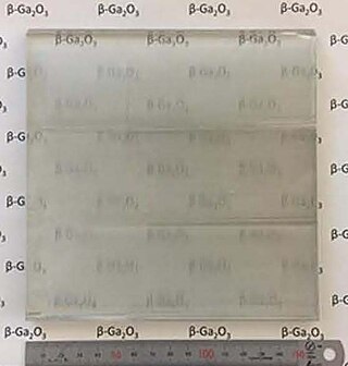
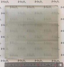
Gallium(III) oxide is an inorganic compound and ultra-wide bandgap semiconductor with the formula Ga2O3. It is actively studied for applications in power electronics, phosphors, and gas sensing. The compound has several polymorphs, of which the monoclinic β-phase is the most stable. The β-phase’s bandgap of 4.7–4.9 eV and large-area, native substrates make it a promising competitor to GaN and SiC-based power electronics applications and solar-blind UV photodetectors. Ga2O3 exhibits reduced thermal conductivity and electron mobility by an order of magnitude compared to GaN and SiC, but is predicted to be significantly more cost-effective due to being the only wide-bandgap material capable of being grown from melt. β-Ga2O3 is thought to be radiation hard which makes it promising for military and space applications.

A quantum dot solar cell (QDSC) is a solar cell design that uses quantum dots as the captivating photovoltaic material. It attempts to replace bulk materials such as silicon, copper indium gallium selenide (CIGS) or cadmium telluride (CdTe). Quantum dots have bandgaps that are adjustable across a wide range of energy levels by changing their size. In bulk materials, the bandgap is fixed by the choice of material(s). This property makes quantum dots attractive for multi-junction solar cells, where a variety of materials are used to improve efficiency by harvesting multiple portions of the solar spectrum.
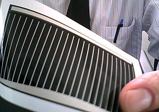
A copper indium gallium selenide solar cell is a thin-film solar cell used to convert sunlight into electric power. It is manufactured by depositing a thin layer of copper indium gallium selenide solution on glass or plastic backing, along with electrodes on the front and back to collect current. Because the material has a high absorption coefficient and strongly absorbs sunlight, a much thinner film is required than of other semiconductor materials.
Band-gap engineering is the process of controlling or altering the band gap of a material. This is typically done to semiconductors by controlling the composition of alloys, constructing layered materials with alternating compositions, or by inducing strain either epitaxially or topologically. A band gap is the range in a solid where no electron state can exist. The band gap of insulators is much larger than in semiconductors. Conductors or metals have a much smaller or nonexistent band gap than semiconductors since the valence and conduction bands overlap. Controlling the band gap allows for the creation of desirable electrical properties.

I-III-VI2 semiconductors are solid semiconducting materials that contain three or more chemical elements belonging to groups I, III and VI (IUPAC groups 1/11, 13 and 16) of the periodic table. They usually involve two metals and one chalcogen. Some of these materials have a direct bandgap, Eg, of approximately 1.5 eV, which makes them efficient absorbers of sunlight and thus potential solar cell materials. A fourth element is often added to a I-III-VI2 material to tune the bandgap for maximum solar cell efficiency. A representative example is copper indium gallium selenide (CuInxGa(1–x)Se2, Eg = 1.7–1.0 eV for x = 0–1), which is used in copper indium gallium selenide solar cells.
Samuel Graham, Jr. is an American engineer and currently the Eugene C. Gwaltney, Jr. School Chair and Professor at Georgia Tech. Graham is a Fellow of the American Society of Mechanical Engineers and serves on the Advisory Board of the Air Force Research Laboratory. On October 1, 2021, he became the Clark School of Engineering dean at the University of Maryland.