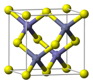
In solid-state physics and solid-state chemistry, a band gap, also called a bandgap or energy gap, is an energy range in a solid where no electronic states exist. In graphs of the electronic band structure of solids, the band gap refers to the energy difference between the top of the valence band and the bottom of the conduction band in insulators and semiconductors. It is the energy required to promote an electron from the valence band to the conduction band. The resulting conduction-band electron are free to move within the crystal lattice and serve as charge carriers to conduct electric current. It is closely related to the HOMO/LUMO gap in chemistry. If the valence band is completely full and the conduction band is completely empty, then electrons cannot move within the solid because there are no available states. If the electrons are not free to move within the crystal lattice, then there is no generated current due to no net charge carrier mobility. However, if some electrons transfer from the valence band to the conduction band, then current can flow. Therefore, the band gap is a major factor determining the electrical conductivity of a solid. Substances having large band gaps are generally insulators, those with small band gaps are semiconductor, and conductors either have very small band gaps or none, because the valence and conduction bands overlap to form a continuous band.

Epitaxy refers to a type of crystal growth or material deposition in which new crystalline layers are formed with one or more well-defined orientations with respect to the crystalline seed layer. The deposited crystalline film is called an epitaxial film or epitaxial layer. The relative orientation(s) of the epitaxial layer to the seed layer is defined in terms of the orientation of the crystal lattice of each material. For most epitaxial growths, the new layer is usually crystalline and each crystallographic domain of the overlayer must have a well-defined orientation relative to the substrate crystal structure. Epitaxy can involve single-crystal structures, although grain-to-grain epitaxy has been observed in granular films. For most technological applications, single domain epitaxy, which is the growth of an overlayer crystal with one well-defined orientation with respect to the substrate crystal, is preferred. Epitaxy can also play an important role while growing superlattice structures.

Molecular-beam epitaxy (MBE) is an epitaxy method for thin-film deposition of single crystals. MBE is widely used in the manufacture of semiconductor devices, including transistors, and it is considered one of the fundamental tools for the development of nanotechnologies. MBE is used to fabricate diodes and MOSFETs at microwave frequencies, and to manufacture the lasers used to read optical discs.
The heterojunction bipolar transistor (HBT) is a type of bipolar junction transistor (BJT) which uses differing semiconductor materials for the emitter and base regions, creating a heterojunction. The HBT improves on the BJT in that it can handle signals of very high frequencies, up to several hundred GHz. It is commonly used in modern ultrafast circuits, mostly radio frequency (RF) systems, and in applications requiring a high power efficiency, such as RF power amplifiers in cellular phones. The idea of employing a heterojunction is as old as the conventional BJT, dating back to a patent from 1951. Detailed theory of heterojunction bipolar transistor was developed by Herbert Kroemer in 1957.

Indium antimonide (InSb) is a crystalline compound made from the elements indium (In) and antimony (Sb). It is a narrow-gap semiconductor material from the III-V group used in infrared detectors, including thermal imaging cameras, FLIR systems, infrared homing missile guidance systems, and in infrared astronomy. Indium antimonide detectors are sensitive to infrared wavelengths between 1 and 5 μm.
Mercury zinc telluride is a telluride of mercury and zinc, an alloy of mercury telluride and zinc telluride. It is a narrow-gap semiconductor material.

A quantum dot solar cell (QDSC) is a solar cell design that uses quantum dots as the captivating photovoltaic material. It attempts to replace bulk materials such as silicon, copper indium gallium selenide (CIGS) or cadmium telluride (CdTe). Quantum dots have bandgaps that are adjustable across a wide range of energy levels by changing their size. In bulk materials, the bandgap is fixed by the choice of material(s). This property makes quantum dots attractive for multi-junction solar cells, where a variety of materials are used to improve efficiency by harvesting multiple portions of the solar spectrum.
Bismuth ferrite (BiFeO3, also commonly referred to as BFO in materials science) is an inorganic chemical compound with perovskite structure and one of the most promising multiferroic materials. The room-temperature phase of BiFeO3 is classed as rhombohedral belonging to the space group R3c. It is synthesized in bulk and thin film form and both its antiferromagnetic (G type ordering) Néel temperature (approximately 653 K) and ferroelectric Curie temperature are well above room temperature (approximately 1100K). Ferroelectric polarization occurs along the pseudocubic direction () with a magnitude of 90–95 μC/cm2.
A quantum well laser is a laser diode in which the active region of the device is so narrow that quantum confinement occurs. Laser diodes are formed in compound semiconductor materials that are able to emit light efficiently. The wavelength of the light emitted by a quantum well laser is determined by the width of the active region rather than just the bandgap of the materials from which it is constructed. This means that much shorter wavelengths can be obtained from quantum well lasers than from conventional laser diodes using a particular semiconductor material. The efficiency of a quantum well laser is also greater than a conventional laser diode due to the stepwise form of its density of states function.

Veeco is a global capital equipment supplier, headquartered in the U.S., that designs and builds processing systems used in semiconductor and compound semiconductor manufacturing, data storage and scientific markets for applications such as advanced packaging, photonics, power electronics and display technologies.
Gertrude Fanny Neumark, also known as Gertrude Neumark Rothschild, was an American physicist, most noted for her work in material science and physics of semiconductors with emphasis on optical and electrical properties of wide-bandgap semiconductors and their light-emitting devices.

Kang Lung Wang is recognized as the discoverer of chiral Majorana fermions by IUPAP. Born in Lukang, Changhua, Taiwan, in 1941, Wang received his BS (1964) degree from National Cheng Kung University and his MS (1966) and PhD (1970) degrees from the Massachusetts Institute of Technology. In 1970 to 1972 he was the Assistant Professor at MIT. From 1972 to 1979, he worked at the General Electric Corporate Research and Development Center as a physicist/engineer. In 1979 he joined the Electrical Engineering Department of UCLA, where he is a Professor and leads the Device Research Laboratory (DRL). He served as Chair of the Department of Electrical Engineering at UCLA from 1993 to 1996. His research activities include semiconductor nano devices, and nanotechnology; self-assembly growth of quantum structures and cooperative assembly of quantum dot arrays Si-based Molecular Beam Epitaxy, quantum structures and devices; Nano-epitaxy of hetero-structures; Spintronics materials and devices; Electron spin and coherence properties of SiGe and InAs quantum structures for implementation of spin-based quantum information; microwave devices. He was the inventor of strained layer MOSFET, quantum SRAM cell, and band-aligned superlattices. He holds 45 patents and published over 700 papers. He is a passionate teacher and has mentored hundreds of students, including MS and PhD candidates. Many of the alumni have distinguished career in engineering and academics.
Band-gap engineering is the process of controlling or altering the band gap of a material. This is typically done to semiconductors by controlling the composition of alloys, constructing layered materials with alternating compositions, or by inducing strain either epitaxially or topologically. A band gap is the range in a solid where no electron state can exist. The band gap of insulators is much larger than in semiconductors. Conductors or metals have a much smaller or nonexistent band gap than semiconductors since the valence and conduction bands overlap. Controlling the band gap allows for the creation of desirable electrical properties.
Cammy R. Abernathy is a materials scientist who is the current dean of the University of Florida's Herbert Wertheim College of Engineering.
Indium aluminium nitride (InAlN) is a direct bandgap semiconductor material used in the manufacture of electronic and photonic devices. It is part of the III-V group of semiconductors, being an alloy of indium nitride and aluminium nitride, and is closely related to the more widely used gallium nitride. It is of special interest in applications requiring good stability and reliability, owing to its large direct bandgap and ability to maintain operation at temperatures of up to 1000 °C., making it of particular interest to areas such as the space industry. InAlN high-electron-mobility transistors (HEMTs) are attractive candidates for such applications owing to the ability of InAlN to lattice-match to gallium nitride, eliminating a reported failure route in the closely related aluminium gallium nitride HEMTs.
Marilyn Gunner is a physics professor at the City College of New York (CUNY) and a Fellow of the American Physical Society. She is known for her work on molecular biophysics and structural biology.
Joanna (Joka) Maria Vandenberg is a Dutch solid state chemist and crystallographer who immigrated to the United States in 1968. At Bell Telephone Laboratories, she made a major contribution to the success of the Internet. She invented, developed, and applied the X-ray scanning tool for quality control essential to manufacturing indium gallium arsenide phosphide-based multi-quantum well lasers. These are the lasers that amplify and modulate light that travels through optical fibers that are at the heart of today's Internet.
Leslie Ann Kolodziejski is an American professor of electrical engineering at the Massachusetts Institute of Technology. She works on fabricating novel photonic devices after synthesizing the constituent material via molecular-beam epitaxy. She is a recipient of the Presidential Young Investigator Award from the National Science Foundation and is a fellow of The Optical Society.

Aristos Christou is an American engineer and scientist, academic professor and researcher. He is a Professor of Materials Science, Professor of Mechanical Engineering and Professor of Reliability Engineering at the University of Maryland.
