Related Research Articles
In integrated circuit manufacturing, photolithography or optical lithography is a general term used for techniques that use light to produce minutely patterned thin films of suitable materials over a substrate, such as a silicon wafer, to protect selected areas of it during subsequent etching, deposition, or implantation operations. Typically, ultraviolet light is used to transfer a geometric design from an optical mask to a light-sensitive chemical (photoresist) coated on the substrate. The photoresist either breaks down or hardens where it is exposed to light. The patterned film is then created by removing the softer parts of the coating with appropriate solvents.

An application-specific integrated circuit is an integrated circuit (IC) chip customized for a particular use, rather than intended for general-purpose use, such as a chip designed to run in a digital voice recorder or a high-efficiency video codec. Application-specific standard product chips are intermediate between ASICs and industry standard integrated circuits like the 7400 series or the 4000 series. ASIC chips are typically fabricated using metal–oxide–semiconductor (MOS) technology, as MOS integrated circuit chips.

Machine vision (MV) is the technology and methods used to provide imaging-based automatic inspection and analysis for such applications as automatic inspection, process control, and robot guidance, usually in industry. Machine vision refers to many technologies, software and hardware products, integrated systems, actions, methods and expertise. Machine vision as a systems engineering discipline can be considered distinct from computer vision, a form of computer science. It attempts to integrate existing technologies in new ways and apply them to solve real world problems. The term is the prevalent one for these functions in industrial automation environments but is also used for these functions in other environment vehicle guidance.
The shadow mask is one of the two technologies used in the manufacture of cathode-ray tube (CRT) televisions and computer monitors which produce clear, focused color images. The other approach is the aperture grille, better known by its trade name, Trinitron. All early color televisions and the majority of CRT computer monitors used shadow mask technology. Both of these technologies are largely obsolete, having been increasingly replaced since the 1990s by the liquid-crystal display (LCD).
Electronic design automation (EDA), also referred to as electronic computer-aided design (ECAD), is a category of software tools for designing electronic systems such as integrated circuits and printed circuit boards. The tools work together in a design flow that chip designers use to design and analyze entire semiconductor chips. Since a modern semiconductor chip can have billions of components, EDA tools are essential for their design; this article in particular describes EDA specifically with respect to integrated circuits (ICs).

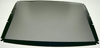
A photomask is an opaque plate with transparent areas that allow light to shine through in a defined pattern. Photomasks are commonly used in photolithography for the production of integrated circuits to produce a pattern on a thin wafer of material. Several masks are used in turn, each one reproducing a layer of the completed design, and together known as a mask set.
CATS is an EDA software for mask data preparation (MDP) in integrated circuit design and manufacturing.
Electron-beam lithography is the practice of scanning a focused beam of electrons to draw custom shapes on a surface covered with an electron-sensitive film called a resist (exposing). The electron beam changes the solubility of the resist, enabling selective removal of either the exposed or non-exposed regions of the resist by immersing it in a solvent (developing). The purpose, as with photolithography, is to create very small structures in the resist that can subsequently be transferred to the substrate material, often by etching.

A smart camera (sensor) or intelligent camera (sensor) or (smart) vision sensor or intelligent vision sensor or smart optical sensor or intelligent optical sensor or smart visual sensor or intelligent visual sensor is a machine vision system which, in addition to image capture circuitry, is capable of extracting application-specific information from the captured images, along with generating event descriptions or making decisions that are used in an intelligent and automated system. A smart camera is a self-contained, standalone vision system with built-in image sensor in the housing of an industrial video camera. The vision system and the image sensor can be integrated into one single piece of hardware known as intelligent image sensor or smart image sensor. It contains all necessary communication interfaces, e.g. Ethernet, as well as industry-proof 24V I/O lines for connection to a PLC, actuators, relays or pneumatic valves, and can be either static or mobile. It is not necessarily larger than an industrial or surveillance camera. A capability in machine vision generally means a degree of development such that these capabilities are ready for use on individual applications. This architecture has the advantage of a more compact volume compared to PC-based vision systems and often achieves lower cost, at the expense of a somewhat simpler (or omitted) user interface. Smart cameras are also referred to by the more general term smart sensors.
Masklesslithography (MPL) is a photomask-less photolithography-like technology used to project or focal-spot write the image pattern onto a chemical resist-coated substrate by means of UV radiation or electron beam.

Extreme ultraviolet lithography is an optical lithography technology used in semiconductor device fabrication to make integrated circuits (ICs). It uses extreme ultraviolet (EUV) wavelengths near 13.5 nm, using a laser-pulsed tin (Sn) droplet plasma, to produce a pattern by using a reflective photomask to expose a substrate covered by photoresist. It is currently applied only in the most advanced semiconductor device fabrication.

A stepper is a device used in the manufacture of integrated circuits (ICs) that is similar in operation to a slide projector or a photographic enlarger. Stepper is short for step-and-repeat camera. Steppers are an essential part of the complex process, called photolithography, which creates millions of microscopic circuit elements on the surface of silicon wafers out of which chips are made. These chips form the heart of ICs such as computer processors, memory chips, and many other devices.

Phase-shift masks are photomasks that take advantage of the interference generated by phase differences to improve image resolution in photolithography. There exist alternating and attenuated phase shift masks. A phase-shift mask relies on the fact that light passing through a transparent media will undergo a phase change as a function of its optical thickness.

Optical proximity correction (OPC) is a photolithography enhancement technique commonly used to compensate for image errors due to diffraction or process effects. The need for OPC is seen mainly in the making of semiconductor devices and is due to the limitations of light to maintain the edge placement integrity of the original design, after processing, into the etched image on the silicon wafer. These projected images appear with irregularities such as line widths that are narrower or wider than designed, these are amenable to compensation by changing the pattern on the photomask used for imaging. Other distortions such as rounded corners are driven by the resolution of the optical imaging tool and are harder to compensate for. Such distortions, if not corrected for, may significantly alter the electrical properties of what was being fabricated. Optical proximity correction corrects these errors by moving edges or adding extra polygons to the pattern written on the photomask. This may be driven by pre-computed look-up tables based on width and spacing between features or by using compact models to dynamically simulate the final pattern and thereby drive the movement of edges, typically broken into sections, to find the best solution,. The objective is to reproduce on the semiconductor wafer, as well as possible, the original layout drawn by the designer.
Digital ICE or Digital Image Correction and Enhancement is a set of technologies related to producing an altered image in a variety of frequency spectra. The objective of these technologies is to render an image more usable by Fourier or other filtering techniques. These technologies were most actively advanced in the 1960s and early 1970s in the fields of strategic reconnaissance and medical electronics.
Resolution enhancement technologies are methods used to modify the photomasks in the lithographic processes used to make integrated circuits to compensate for limitations in the optical resolution of the projection systems. These processes allow the creation of features well beyond the limit that would normally apply due to the Rayleigh criterion. Modern technologies allow the creation of features on the order of 5 nanometers (nm), far below the normal resolution possible using deep ultraviolet (DUV) light.
Design Closure is a part of the digital electronic design automation workflow by which an integrated circuit design is modified from its initial description to meet a growing list of design constraints and objectives.
Contact lithography, also known as contact printing, is a form of photolithography whereby the image to be printed is obtained by illumination of a photomask in direct contact with a substrate coated with an imaging photoresist layer.
Automated X-ray inspection (AXI) is a technology based on the same principles as automated optical inspection (AOI). It uses X-rays as its source, instead of visible light, to automatically inspect features, which are typically hidden from view.
An aligner, or mask aligner, is a system that produces integrated circuits (IC) using the photolithography process. It holds the photomask over the silicon wafer while a bright light is shone through the mask and onto the photoresist. The "alignment" refers to the ability to place the mask over precisely the same location repeatedly as the chip goes through multiple rounds of lithography. Aligners were a major part of IC manufacture from the 1960s into the late 1970s, when they began to be replaced by the stepper.
References
- ↑ "VLSI technology: fundamentals and applications", by Yasuo Tarui, 1986, ISBN 3-540-12558-2, Chapter 4: "Mask Inspection Technology"
- ↑ ZEISS Webpage offering automated mask repair tools
- ↑ "Design for manufacturability and yield for nano-scale CMOS", by Charles Chiang, Jamil Kawa, 2007, ISBN 1-4020-5187-5, p. 237
| | This electronics-related article is a stub. You can help Wikipedia by expanding it. |