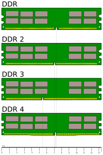
Double Data Rate Synchronous Dynamic Random-Access Memory is a double data rate (DDR) synchronous dynamic random-access memory (SDRAM) class of memory integrated circuits used in computers. DDR SDRAM, also retroactively called DDR1 SDRAM, has been superseded by DDR2 SDRAM, DDR3 SDRAM, DDR4 SDRAM and DDR5 SDRAM. None of its successors are forward or backward compatible with DDR1 SDRAM, meaning DDR2, DDR3, DDR4 and DDR5 memory modules will not work in DDR1-equipped motherboards, and vice versa.

Celeron is Intel's brand name for low-end IA-32 and x86-64 computer microprocessor models targeted at low-cost personal computers.

Synchronous dynamic random-access memory is any DRAM where the operation of its external pin interface is coordinated by an externally supplied clock signal.
Rambus DRAM (RDRAM), and its successors Concurrent Rambus DRAM (CRDRAM) and Direct Rambus DRAM (DRDRAM), are types of synchronous dynamic random-access memory (SDRAM) developed by Rambus from the 1990s through to the early-2000s. The third-generation of Rambus DRAM, DRDRAM was replaced by XDR DRAM. Rambus DRAM was developed for high-bandwidth applications, and was positioned by Rambus as replacement for various types of contemporary memories, such as SDRAM.
HyperTransport (HT), formerly known as Lightning Data Transport (LDT), is a technology for interconnection of computer processors. It is a bidirectional serial/parallel high-bandwidth, low-latency point-to-point link that was introduced on April 2, 2001. The HyperTransport Consortium is in charge of promoting and developing HyperTransport technology.

Pentium 4 is a series of single-core CPUs for desktops, laptops and entry-level servers manufactured by Intel. The processors were shipped from November 20, 2000 until August 8, 2008. The production of Netburst processors was active from 2000 until May 21, 2010.

In computing, overclocking is the practice of increasing the clock rate of a computer to exceed that certified by the manufacturer. Commonly, operating voltage is also increased to maintain a component's operational stability at accelerated speeds. Semiconductor devices operated at higher frequencies and voltages increase power consumption and heat. An overclocked device may be unreliable or fail completely if the additional heat load is not removed or power delivery components cannot meet increased power demands. Many device warranties state that overclocking or over-specification voids any warranty, however there are an increasing number of manufacturers that will allow overclocking as long as performed (relatively) safely.

A front-side bus (FSB) is a computer communication interface (bus) that was often used in Intel-chip-based computers during the 1990s and 2000s. The EV6 bus served the same function for competing AMD CPUs. Both typically carry data between the central processing unit (CPU) and a memory controller hub, known as the northbridge.
Slot 1 refers to the physical and electrical specification for the connector used by some of Intel's microprocessors, including the Pentium Pro, Celeron, Pentium II and the Pentium III. Both single and dual processor configurations were implemented.

In computing, a northbridge is one of two chips comprising the core logic chipset architecture on a PC motherboard. A northbridge is connected directly to a CPU via the front-side bus (FSB) to handle high-performance tasks, and is usually used in conjunction with a slower southbridge to manage communication between the CPU and other parts of the motherboard. Since the 2010s, die shrink and improved transistor density have allowed for increasing chipset integration, and the functions performed by northbridges are now often incorporated into other components. As of 2019, Intel and AMD had both released chipsets in which all northbridge functions had been integrated into the CPU. Modern Intel Core processors have the northbridge integrated on the CPU die, where it is known as the uncore or system agent.
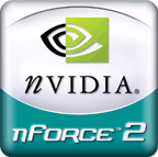
The nForce2 chipset was released by Nvidia in July 2002 as a refresh to the original nForce product offering. The nForce2 chipset was a platform for motherboards supporting AMD's Socket A CPUs along with DDR SDRAM. There were variations of the chipset including one with and one without an integrated GeForce4 MX graphics processor (IGP).
Double Data Rate 3 Synchronous Dynamic Random-Access Memory is a type of synchronous dynamic random-access memory (SDRAM) with a high bandwidth interface, and has been in use since 2007. It is the higher-speed successor to DDR and DDR2 and predecessor to DDR4 synchronous dynamic random-access memory (SDRAM) chips. DDR3 SDRAM is neither forward nor backward compatible with any earlier type of random-access memory (RAM) because of different signaling voltages, timings, and other factors.

The Intel 440BX is a chipset from Intel, supporting Pentium II, Pentium III, and Celeron processors. It is also known as the i440BX and was released in April 1998. The official part number is 82443BX.

In computing, the clock multiplier sets the ratio of an internal CPU clock rate to the externally supplied clock. A CPU with a 10x multiplier will thus see 10 internal cycles for every external clock cycle. For example, a system with an external clock of 100 MHz and a 36x clock multiplier will have an internal CPU clock of 3.6 GHz. The external address and data buses of the CPU also use the external clock as a fundamental timing base; however, they could also employ a (small) multiple of this base frequency to transfer data faster.

Pumping, when referring to computer systems, is an informal term for transmitting a data signal more than one time per clock signal.
The AMD 700 chipset series is a set of chipsets designed by ATI for AMD Phenom processors to be sold under the AMD brand. Several members were launched in the end of 2007 and the first half of 2008, others launched throughout the rest of 2008.
Intel's Skulltrail is an enthusiast gaming platform that was released on February 19, 2008. It is based on the company's 5400 "Seaburg" workstation chipset. The primary difference between Skulltrail and Intel's current and past enthusiast chipsets is a dual CPU socket design that allows two processors to operate on the same motherboard. Therefore, Skulltrail can operate eight processing cores on one system. The platform supports two Core 2 Extreme QX9775 processors, which operate at 3.2 GHz.

Phenom II is a family of AMD's multi-core 45 nm processors using the AMD K10 microarchitecture, succeeding the original Phenom. Advanced Micro Devices released the Socket AM2+ version of Phenom II in December 2008, while Socket AM3 versions with DDR3 support, along with an initial batch of triple- and quad-core processors were released on February 9, 2009. Dual-processor systems require Socket F+ for the Quad FX platform. The next-generation Phenom II X6 was released on April 27, 2010.

The Intel 850 chipset was the first chipset available for the Pentium 4 processor, and was simultaneously released in November 2000. It consists of an 82850 memory controller hub and an 82801BA I/O controller hub.

Skylake is the codename used by Intel for a processor microarchitecture that was launched in August 2015 succeeding the Broadwell microarchitecture. Skylake is a microarchitecture redesign using the same 14 nm manufacturing process technology as its predecessor, serving as a tock in Intel's tick–tock manufacturing and design model. According to Intel, the redesign brings greater CPU and GPU performance and reduced power consumption. Skylake CPUs share their microarchitecture with Kaby Lake, Coffee Lake, Cannon Lake, Whiskey Lake, and Comet Lake CPUs.