
Chemical vapor deposition (CVD) is a vacuum deposition method used to produce high-quality, and high-performance, solid materials. The process is often used in the semiconductor industry to produce thin films.

MEMS is the technology of microscopic devices incorporating both electronic and moving parts. MEMS are made up of components between 1 and 100 micrometres in size, and MEMS devices generally range in size from 20 micrometres to a millimetre, although components arranged in arrays can be more than 1000 mm2. They usually consist of a central unit that processes data and several components that interact with the surroundings.
Solid-state chemistry, also sometimes referred as materials chemistry, is the study of the synthesis, structure, and properties of solid phase materials. It therefore has a strong overlap with solid-state physics, mineralogy, crystallography, ceramics, metallurgy, thermodynamics, materials science and electronics with a focus on the synthesis of novel materials and their characterization. A diverse range of synthetic techniques, such as the ceramic method and chemical vapour depostion, make solid-state materials. Solids can be classified as crystalline or amorphous on basis of the nature of order present in the arrangement of their constituent particles. Their elemental compositions, microstructures, and physical properties can be characterized through a variety of analytical methods.

Silane (Silicane) is an inorganic compound with chemical formula SiH4. It is a colorless, pyrophoric, toxic gas with a sharp, repulsive, pungent smell, somewhat similar to that of acetic acid. Silane is of practical interest as a precursor to elemental silicon. Silane with alkyl groups are effective water repellents for mineral surfaces such as concrete and masonry. Silanes with both organic and inorganic attachments are used as coupling agents. They are commonly used to apply coatings to surfaces or as an adhesion promoter.
A thin film is a layer of materials ranging from fractions of a nanometer (monolayer) to several micrometers in thickness. The controlled synthesis of materials as thin films is a fundamental step in many applications. A familiar example is the household mirror, which typically has a thin metal coating on the back of a sheet of glass to form a reflective interface. The process of silvering was once commonly used to produce mirrors, while more recently the metal layer is deposited using techniques such as sputtering. Advances in thin film deposition techniques during the 20th century have enabled a wide range of technological breakthroughs in areas such as magnetic recording media, electronic semiconductor devices, integrated passive devices, light-emitting diodes, optical coatings, hard coatings on cutting tools, and for both energy generation and storage. It is also being applied to pharmaceuticals, via thin-film drug delivery. A stack of thin films is called a multilayer.

Heterogeneous catalysis is catalysis where the phase of catalysts differs from that of the reagents or products. The process contrasts with homogeneous catalysis where the reagents, products and catalyst exist in the same phase. Phase distinguishes between not only solid, liquid, and gas components, but also immiscible mixtures, or anywhere an interface is present.

Self-assembled monolayers (SAM) of organic molecules are molecular assemblies formed spontaneously on surfaces by adsorption and are organized into more or less large ordered domains. In some cases molecules that form the monolayer do not interact strongly with the substrate. This is the case for instance of the two-dimensional supramolecular networks of e.g. perylenetetracarboxylic dianhydride (PTCDA) on gold or of e.g. porphyrins on highly oriented pyrolitic graphite (HOPG). In other cases the molecules possess a head group that has a strong affinity to the substrate and anchors the molecule to it. Such a SAM consisting of a head group, tail and functional end group is depicted in Figure 1. Common head groups include thiols, silanes, phosphonates, etc.
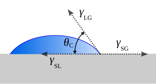
The contact angle is the angle between a liquid surface and a solid surface where they meet. More specifically, it is the angle between the surface tangent on the liquid–vapor interface and the tangent on the solid–liquid interface at their intersection. It quantifies the wettability of a solid surface by a liquid via the Young equation.

Matrix isolation is an experimental technique used in chemistry and physics. It generally involves a material being trapped within an unreactive matrix. A host matrix is a continuous solid phase in which guest particles are embedded. The guest is said to be isolated within the host matrix. Initially the term matrix-isolation was used to describe the placing of a chemical species in any unreactive material, often polymers or resins, but more recently has referred specifically to gases in low-temperature solids. A typical matrix isolation experiment involves a guest sample being diluted in the gas phase with the host material, usually a noble gas or nitrogen. This mixture is then deposited on a window that is cooled to below the melting point of the host gas. The sample may then be studied using various spectroscopic procedures.

Metalorganic vapour-phase epitaxy (MOVPE), also known as organometallic vapour-phase epitaxy (OMVPE) or metalorganic chemical vapour deposition (MOCVD), is a chemical vapour deposition method used to produce single- or polycrystalline thin films. It is a process for growing crystalline layers to create complex semiconductor multilayer structures. In contrast to molecular-beam epitaxy (MBE), the growth of crystals is by chemical reaction and not physical deposition. This takes place not in vacuum, but from the gas phase at moderate pressures. As such, this technique is preferred for the formation of devices incorporating thermodynamically metastable alloys, and it has become a major process in the manufacture of optoelectronics, such as light-emitting diodes, its most widespread application. It was first demonstrated in 1967 at North American Aviation Autonetics Division in Anaheim CA by Harold M. Manasevit.
Chemical beam epitaxy (CBE) forms an important class of deposition techniques for semiconductor layer systems, especially III-V semiconductor systems. This form of epitaxial growth is performed in an ultrahigh vacuum system. The reactants are in the form of molecular beams of reactive gases, typically as the hydride or a metalorganic. The term CBE is often used interchangeably with metal-organic molecular beam epitaxy (MOMBE). The nomenclature does differentiate between the two processes, however. When used in the strictest sense, CBE refers to the technique in which both components are obtained from gaseous sources, while MOMBE refers to the technique in which the group III component is obtained from a gaseous source and the group V component from a solid source.
Atomic layer deposition (ALD) is a thin-film deposition technique based on the sequential use of a gas-phase chemical process; it is a subclass of chemical vapour deposition. The majority of ALD reactions use two chemicals called precursors. These precursors react with the surface of a material one at a time in a sequential, self-limiting, manner. A thin film is slowly deposited through repeated exposure to separate precursors. ALD is a key process in fabricating semiconductor devices, and part of the set of tools for synthesizing nanomaterials.

Parylene is the common name of a polymer whose backbone consists of para-benzenediyl rings −C
6H
4− connected by 1,2-ethanediyl bridges −CH
2−CH
2−. It can be obtained by polymerization of para-xylyleneH
2C=C
6H
4=CH
2.
Silanization is the attachment of an organosilyl group to some chemical species. Almost always, silanization is the conversion of a silanol-terminated surface to a alkylsiloxy-terminated surface. This conversion confers hydrophobicity to a previously hydrophilic surface. This process is often used to modify the surface properties of glass, silicon, alumina, quartz, and metal oxide substrates, which all have an abundance of hydroxyl groups. Silanization differs from silylation, which usually refers to attachment of organosilicon groups to molecular substrates.
Plasma polymerization uses plasma sources to generate a gas discharge that provides energy to activate or fragment gaseous or liquid monomer, often containing a vinyl group, in order to initiate polymerization. Polymers formed from this technique are generally highly branched and highly cross-linked, and adhere to solid surfaces well. The biggest advantage to this process is that polymers can be directly attached to a desired surface while the chains are growing, which reduces steps necessary for other coating processes such as grafting. This is very useful for pinhole-free coatings of 100 picometers to 1-micrometer thickness with solvent insoluble polymers.
Silanization of silicon and mica is the coating of these materials with a thin layer of self assembling units.
Perfluorodecyltrichlorosilane, also known as FDTS, is a colorless liquid chemical with molecular formula C10H4Cl3F17Si. FDTS molecules form self-assembled monolayers. They form covalent silicon–oxygen bonds to free hydroxyl (–OH) groups, such as the surfaces of glass, ceramics, or silica.
Molecular layer deposition (MLD) is a vapour phase thin film deposition technique based on self-limiting surface reactions carried out in a sequential manner. Essentially, MLD resembles the well established technique of atomic layer deposition (ALD) but, whereas ALD is limited to exclusively inorganic coatings, the precursor chemistry in MLD can use small, bifunctional organic molecules as well. This enables, as well as the growth of organic layers in a process similar to polymerization, the linking of both types of building blocks together in a controlled way to build up organic-inorganic hybrid materials.
Sequential infiltration synthesis (SIS) is a technique derived from atomic layer deposition (ALD) in which a polymer is infused with inorganic material using sequential, self-limiting exposures to gaseous precursors, enabling precise manipulation over the composition, structure, and properties. The technique has applications in fields such as nanotechnology, materials science, and electronics, where precise material engineering is required.