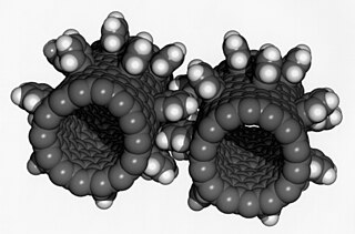
Nanotechnology was defined by the National Nanotechnology Initiative as the manipulation of matter with at least one dimension sized from 1 to 100 nanometers (nm). At this scale, commonly known as the nanoscale, surface area and quantum mechanical effects become important in describing properties of matter. The definition of nanotechnology is inclusive of all types of research and technologies that deal with these special properties. It is therefore common to see the plural form "nanotechnologies" as well as "nanoscale technologies" to refer to the broad range of research and applications whose common trait is size. An earlier description of nanotechnology referred to the particular technological goal of precisely manipulating atoms and molecules for fabrication of macroscale products, also now referred to as molecular nanotechnology.
Nanoengineering is the practice of engineering on the nanoscale. It derives its name from the nanometre, a unit of measurement equalling one billionth of a meter.
Scanning probe microscopy (SPM) is a branch of microscopy that forms images of surfaces using a physical probe that scans the specimen. SPM was founded in 1981, with the invention of the scanning tunneling microscope, an instrument for imaging surfaces at the atomic level. The first successful scanning tunneling microscope experiment was done by Gerd Binnig and Heinrich Rohrer. The key to their success was using a feedback loop to regulate gap distance between the sample and the probe.

James Kazimierz Gimzewski FRS FREng FInstP is a Scottish physicist of Polish descent who pioneered research on electrical contacts with single atoms and molecules and light emission using scanning tunneling microscopy (STM).
A nanoruler is a tool or a method used within the subfield of "nanometrology" to achieve precise control and measurements at the nanoscale. Measurements of extremely tiny proportions require more complicated procedures, such as manipulating the properties of light (plasmonic) or DNA to determine distances. At the nanoscale, materials and devices exhibit unique properties that can significantly influence their behavior. In fields like electronics, medicine, and biotechnology, where advancements come from manipulating matter at the atomic and molecular levels, nanoscale measurements become essential.
Nanolithography (NL) is a growing field of techniques within nanotechnology dealing with the engineering of nanometer-scale structures on various materials.

Focused ion beam, also known as FIB, is a technique used particularly in the semiconductor industry, materials science and increasingly in the biological field for site-specific analysis, deposition, and ablation of materials. A FIB setup is a scientific instrument that resembles a scanning electron microscope (SEM). However, while the SEM uses a focused beam of electrons to image the sample in the chamber, a FIB setup uses a focused beam of ions instead. FIB can also be incorporated in a system with both electron and ion beam columns, allowing the same feature to be investigated using either of the beams. FIB should not be confused with using a beam of focused ions for direct write lithography. These are generally quite different systems where the material is modified by other mechanisms.

Near-field scanning optical microscopy (NSOM) or scanning near-field optical microscopy (SNOM) is a microscopy technique for nanostructure investigation that breaks the far field resolution limit by exploiting the properties of evanescent waves. In SNOM, the excitation laser light is focused through an aperture with a diameter smaller than the excitation wavelength, resulting in an evanescent field on the far side of the aperture. When the sample is scanned at a small distance below the aperture, the optical resolution of transmitted or reflected light is limited only by the diameter of the aperture. In particular, lateral resolution of 6 nm and vertical resolution of 2–5 nm have been demonstrated.
Nanophotonics or nano-optics is the study of the behavior of light on the nanometer scale, and of the interaction of nanometer-scale objects with light. It is a branch of optics, optical engineering, electrical engineering, and nanotechnology. It often involves dielectric structures such as nanoantennas, or metallic components, which can transport and focus light via surface plasmon polaritons.

Nanochemistry is an emerging sub-discipline of the chemical and material sciences that deals with the development of new methods for creating nanoscale materials. The term "nanochemistry" was first used by Ozin in 1992 as 'the uses of chemical synthesis to reproducibly afford nanomaterials from the atom "up", contrary to the nanoengineering and nanophysics approach that operates from the bulk "down"'. Nanochemistry focuses on solid-state chemistry that emphasizes synthesis of building blocks that are dependent on size, surface, shape, and defect properties, rather than the actual production of matter. Atomic and molecular properties mainly deal with the degrees of freedom of atoms in the periodic table. However, nanochemistry introduced other degrees of freedom that controls material's behaviors by transformation into solutions. Nanoscale objects exhibit novel material properties, largely as a consequence of their finite small size. Several chemical modifications on nanometer-scaled structures approve size dependent effects.
Electron-beam-induced deposition (EBID) is a process of decomposing gaseous molecules by an electron beam leading to deposition of non-volatile fragments onto a nearby substrate. The electron beam is usually provided by a scanning electron microscope, which results in high spatial accuracy and the possibility to produce free-standing, three-dimensional structures.

Nanometrology is a subfield of metrology, concerned with the science of measurement at the nanoscale level. Nanometrology has a crucial role in order to produce nanomaterials and devices with a high degree of accuracy and reliability in nanomanufacturing.
The following outline is provided as an overview of and topical guide to nanotechnology:

Local oxidation nanolithography (LON) is a tip-based nanofabrication method. It is based on the spatial confinement on an oxidation reaction under the sharp tip of an atomic force microscope.
A recurrence tracking microscope (RTM) is a microscope that is based on the quantum recurrence phenomenon of an atomic wave packet. It is used to investigate the nano-structure on a surface.
Nanochannel glass materials are an experimental mask technology that is an alternate method for fabricating nanostructures, although optical lithography is the predominant patterning technique.

A Boy and His Atom is a 2013 stop-motion animated short film released on YouTube by IBM Research. One minute in length, it was made by moving carbon monoxide molecules with a scanning tunneling microscope, a device that magnifies them 100 million times. These two-atom molecules were moved to create images, which were then saved as individual frames to make the film. The movie was recognized by the Guinness Book of World Records as the World's Smallest Stop-Motion Film in 2013.

Victoria Vesna is a professor and digital media artist. She is known for her feminist video, computer and internet art and has been active since the early 1980s. Along with collaborator Jim Gimzewski she is thought to have created one of the first interactive artworks related to nanotechnology and defines her art practice as experimental research.
A probe tip is an instrument used in scanning probe microscopes (SPMs) to scan the surface of a sample and make nano-scale images of surfaces and structures. The probe tip is mounted on the end of a cantilever and can be as sharp as a single atom. In microscopy, probe tip geometry and the composition of both the tip and the surface being probed directly affect resolution and imaging quality. Tip size and shape are extremely important in monitoring and detecting interactions between surfaces. SPMs can precisely measure electrostatic forces, magnetic forces, chemical bonding, Van der Waals forces, and capillary forces. SPMs can also reveal the morphology and topography of a surface.
This glossary of nanotechnology is a list of definitions of terms and concepts relevant to nanotechnology, its sub-disciplines, and related fields.

