Nanofluidic circuitry is a nanotechnology aiming for control of fluids in nanometer scale. Due to the effect of an electrical double layer within the fluid channel, the behavior of nanofluid is observed to be significantly different compared with its microfluidic counterparts. Its typical characteristic dimensions fall within the range of 1–100nm. At least one dimension of the structure is in nanoscopic scale. Phenomena of fluids in nano-scale structure are discovered to be of different properties in electrochemistry and fluid dynamics.
With the development of microfabrication and nanotechnology, the study of microfluidics and nanofluidics is drawing more attention.[1] Research on microfluidic found its advantages in DNA analysis, lab-on-a-chip, and micro-TAS. Devices in a microfluidic system include channels, valves, mixers, and pumps. Integration of these microfluidic devices enables sorting, transporting, and mixing of substances within fluids. However, the failure of moving parts in these systems is usually the critical issue and the main drawback. Mechanisms to control flow without using mechanical parts are always desired for reliability and lifetime.[2]
In 1997, Wei, Bard and Feldberg discovered that ion rectification occurs at the tip of a nano-sized pipe.[3] They observed that the surface charge at the wall of a nano-pipet induced a non-neutral electrical potential within the orifice. The electrical potential then modifies the concentration of ion species, resulting in an asymmetric current-voltage characteristic for the current through the pipet.
Transport of ions in the electrolyte can be adjusted by tuning the pH value in a dilute ionic solution, or by introducing an external electrical potential to change the surface charge density of the wall.[4] As an analogy to semiconductor devices, the mechanism to control charge carrier transport in electronic devices was established in the area of nanofluidics. In nanofluidics, the active control of ion transport is realized using nano-scale channels or pores.
Research efforts on micro-scaled fluidic systems started to focus on the rectifying phenomena, which can be seen only in nano-scaled systems. In 2006, Professor Majumdar and Professor Yang in University of California, Berkeley built the first "nanofluidic" transistor. The transistor can be turn on or off by an external electrical signal, allowing the control of ionic fluids in a nano-scaled channel. Their work implies a possibility to create a nanofluidic circuitry with logic functions.
The main researchers in the area of nanofluidic devices include Arun Majumdar and Peidong Yang in University of California - Berkeley, Harold Craighead and Brian Kirbyat Cornell University, Juan Santiago at Stanford University, Albert van den Berg in University of Twente, Zuzanna Siwy in University of California - Irvine, and Mark Shannon in University of Illinois - Urbana-Champaign.
Basic principles
For electrolyte solution in a channel with a macro- or micro-scaled radius, surface charges at the wall attract counterions and repel co-ions due to electrostatic force. Therefore, an electrical double layer exists between the wall of channel and the solution. The dimension of the electrical double layer is determined by the Debye length in this system, which is typically much smaller than the channel radius. Most of the solution in the channel is electrically neutral due to the shielding effect of the electrical double layer.
In a nanochannel, however, the solution is charged when the dimension of channel radius is smaller than the Debye length. Therefore, it is possible to manipulate the flow of ions inside the nanochannel by introducing surface charges on the wall or by applying an external electrical potential.
Ionic concentration of solution has an important effect on the ion transport. Because a higher concentration leads to a shorter Debye length for the electrical double layer at the channel wall. Its rectifying effect decreases with increasing ionic concentration. On the other hand, ion rectification can be improved by having a dilute solution.
Ion transport
To analyze the transport of ions in the channel, behaviors of system in electrochemistry as well as fluid mechanics need to be considered. The Poisson–Nernst–Planck (PNP) equations are utilized to describe ionic current flowing through a channel, and the Navier–Stokes (NS) equations are used to represent the fluid dynamics in the channel.
where is the electrostatic potential, is the unit charge of electron, is the permittivity in vacuum, and is the dielectric constant of solution; , and are the diffusivity, the number density of ions, and the valence of ion species .
The solution in steady-state satisfies the continuity equation. To describe fluid velocity field in the channel, using Navier–Stokes equations:
where , , , and are pressure, velocity vector, viscosity, and density of fluid, respectively. The equations above are usually solved with numerical algorithm to determine the velocity, pressure, electric potential, and ionic concentration in the fluid, as well as the electric current flow through the channel.
Ionic selectivity
Ionic selectivity is defined to evaluate the performance of a nano-channel for ionic flow control.[7] Ionic selectivity is the ratio of the difference in currents of majority and minority carriers to the total current carried by both positive and negative ions, . For a nanochannel with perfect control over cation and anion, the selectivity is unity. For a nanochannel without ionic flow control, the selectivity is zero.
Nanofluidic logic devices
Transport is proportional to applied bias (resistor)
Transport can be made to move in one direction (diode)
Control of gain is possible by introduction of third pole (transistor)
Control of the forward/reverse direction by asymmetric gates (Field-effect reconfigurable diode)
Diodes
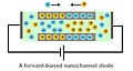
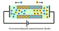
Nanofluidic diodes are utilized for rectification of ionic transport.[8][9][10] A diode in electronic circuits limits the flow of electric current to one direction. A nanofluidic diode has the same function to restrict the ionic flow in one direction. A nanofluidic diode is a channel with its radius dimension of several nanometers. The inner surface of the channel is coated with surface charges. Current rectification can occur when the surface charges at the wall are of the same sign. It is also observed that, when a half of the channel is coated with opposite sign or electrically neutral, the rectification will be enhanced.
When the wall of the channel is coated with positive charges, the negative charged ions in the electrolyte will be attracted and accumulated within the channel. In this case, the flow of positive charges passing through the channel is not favorable, resulting in a decrease in ionic current. Therefore, the ionic current becomes asymmetric if the biasing voltage is reversed.
A forward-biased nanofluidic diode
A reverse-biased nanofluidic diode
Field-effect transistors
By applying an additional electrode on a nanochannel as the gate electrode, it is possible to adjust the electrical potential inside the channel.[11][12] A nanofluidic field-effect transistor can be made of silica nanotubes with an oxide as the dielectric material between the metal gate electrode and the channel.[13] The tuning of the ionic current, therefore, can be achieved by changing the voltage applied on the gate. The gate bias and the source-drain bias are applied to adjust the cation and anion concentration within the nanochannel, therefore tuning the ionic current flowing through it.[14]
This concept is an analogy to the structure of a metal-oxide semiconductor field-effect transistor (MOSFET) in electronic circuits. Similar to a MOSFET, a nanofluidic transistor is the fundamental element for building a nanofluidic circuitry. There is possibility to achieve a nanofluidic circuitry, which is capable of logic operation and manipulation for ionic particles.
Since the conductance of ionic current flow is controlled by the gate voltage, using a material with high dielectric constant as the wall of the channel is desired. In this case, there is a stronger field seen within the channel due to a higher gate capacitance. A channel surface with a low surface charge is also desired in order to strengthen the effect of potential tuning by gate electrode. This increases the ability to spatially and temporally tune the ionic and electrostatic environment in the channel.
By introducing an asymmetric field effect along the nanochannel, a field-effect reconfigurable nanofluidic diode is feasible,[16] which features post-fabrication reconfiguration of the diode functions, such as the forward/reverse directions and the rectification degrees. Unlike the nanofluidic field-effect transistor, where only the amount of ions/molecules is regulated by an electrostatic potential, the field-effect reconfigurable diode can be used to control both directions and magnitudes of ion/molecule transport. This device could be deemed as the building blocks for ionic counterpart of the electronic field-programmable gate array.
Ionic bipolar transistors
Ionic bipolar transistors can be made from two conical channels with the smallest opening in nano-scaled dimension. By introducing opposite surface charges at each side, it is able to rectify ionic current as an ionic diode. An ionic bipolar transistor is built by combining two ionic diodes and forming a PNP junction along the inner surface of the channel. While the ionic current is from emitter end to collector end, the strength of the current can be modulated by the base electrode. The surface charge at the channel wall can be modified using chemical methods, by changing the electrolyte concentration or pH value.
Ionic triodes
Nanofuidic triode is a three-terminal double junction nanofluidic device composed of positive-charged alumina and negative-charged silica nanochannels.[17] The device is essentially a three-terminal bipolar junction transistor. By controlling the voltage across emitter and collector terminals, one can regulate the ion current from base terminal to one of the other two terminals, functioning as an ionic single-pole, double-throw switch.
Size effect of nanostructures
Width of nanochannels
When surface charges present at the wall of a channel of micro-scaled width, counterions are attracted and co-ions are repelled by electrostatic force. The counterions form a shielding area near the wall. This region penetrate into solution to a certain distance called Debye length until the electric potential decays to the bulk value of neutrality. The Debye length is ranging typically from 1nm to 100nm for aqueous solutions.
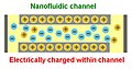
In nano-channels, the Debye length is usually comparable with the channel width, therefore solution within the channel is charged. Ions inside the fluid is no longer shielded from surface charge. Instead, surface charge affect the dynamics of ions within a nano-channel.
Microfluidic channel, electrically neutral inside the channel[18]
Nanofluidic channel, electrically charged inside the channel
Length of nanochannels
It requires a channel to be narrow and long for it to have a good selectivity. In other words, a channel with a high aspect ratio has a better selectivity. To further increase its selectivity, it is required to have a highly charged wall.[7]
The performance of ionic selectivity also largely related to the applied bias. With a low bias, a high selectivity is observed. With the increase of the bias voltage, there is an apparent decrease in the selectivity. For a nanochannel with a low aspect ratio, high selectivity is possible when the bias voltage is low.
Long channel and low bias voltage result in high selectivity
Short channel and high bias voltage result in low selectivity
Fabrication
The advantage of nanofluidic devices is from its feasibility to be integrated with electronic circuitry. Because they are built using the same manufacturing technology, it is possible to make a nanofluidic system with digital integrated circuit on a single chip. Therefore, the control and manipulation of particles in the electrolyte can be achieved in a real-time.[19]
Fabrication of nano-channels is categorized into top-down and bottom-up methods. Top-down methods are the conventional processes utilized in the IC industry and Microelectromechanical systems research. It begins with photolithography on a bulk silicon wafer. Bottom-up methods, in contrast, starts with atoms or molecules with intrinsic nano-scaled dimension. By organize and combine these building blocks together, it is able to form a nanostructures as small as only a few nanometers.
Top-down methods
A typical method of top-down fabrication includes photolithography to define the geometry of channels on a substrate wafer. The geometry is created by several thin-film deposition and etching steps to form trenches. The substrate wafer is then bonded to another wafer to seal the trenches and form channels. Other technologies to fabricate nano-channels include surface micromachining with sacrificial layers, nano-imprinting lithography, and soft-lithography.
Bottom-up methods
The most common method utilized for bottom-up fabrication is self-assembled monolayers (SAM). This method usually use biological materials to form a molecular monolayer on the substrate. Nano-channels can also be fabricated from the growth of carbon nanotubes (CNT) and quantum wires. The bottom-up methods usually give well-defined shapes with characteristic length about few nanometers. For these structures to be utilized as nanofluidic devices, the interconnection between nano-channels and microfluidic systems becomes an important issue.
There exist several ways to coat the inner surface with specific charges. Diffusion-limited patterning can be utilized because a bulk solution only penetrate the entrance of a nanochannel within a certain distance. Because the diffusion speed is different for each reactant. By introducing several steps of reactants flowing into the nanochannel, it is possible to pattern the surface with different surface charges inside the channel.[20]
Application
Nanofluidic devices have been built for application in chemistry, molecular biology and medicine. The main purposes to use nanofluidic devices are separation and measurement of solutions containing nanoparticles for drug delivery, gene therapy and nanoparticle toxicology on a micro-total-analysis system.[21] An important advantage of micro- and nano-scaled systems is the small amount of sample or reagent used in analysis. This reduces the time required for sample processing. It is also possible to achieve analysis in an array, which further speeds up processes and increases throughput of analysis.
Nanochannels are utilized to achieve single-molecule sensing and diagnosis, as well as DNA separation. In many cases, nanofluidic devices are integrated within a microfluidic system to facilitate logic operation of fluids. The future of nanofluidic systems will be focused on several areas such as analytical chemistry and biochemistry, liquid transport and metering, and energy conversion.
In nanofluidics, the valence numbers of the ions determines their net electrophoretic velocities. In other words, the velocity of an ion in the nano-channel is related not only to its ion mobility but also its ion valence. This enables the sorting function of nanofluidics, which cannot be done in a micro-channel. Therefore, it is possible to do sorting and separation for short strand DNA by using a nanochannel. For the single-molecule DNA application, the final goal is to sequence a strand of genomic DNA in a reproducible and precise result. Similar application can also be found in chromatography, or separation of various ingredients in the solution.
Application also can be found in synthesis of fibers. Polymer fibers can be created by electrospinning the monomers at an interface between liquid and vacuum. An organized polymer structure is formed from a flow of monomers aligning on a substrate.
There is also an attempt to bring nanofluidic technology into energy conversion. In this case, the electrical charged wall behaves as the stator, while the flowing solution as the rotor. It is observed that when the pressure-driven solvent flowing through a charged nanochannel, it can generate a streaming current and a streaming potential. This phenomenon can be used in electrical energy harvesting.
Advances in nanofabrication techniques and concerns about energy shortage make people interested in this idea. The main challenge is to increase efficiency, which is now only a few percent, compared with efficiencies of up to about 95 per cent for standard rotational electromagnetic generators.
Recent advancements
Recent studies focus on the integration of nanofluidic devices into microsystems. An interface should be created for the connection between two length-scales. A system with solely nanofluidic devices standalone is impractical because it would requires a large driving pressure to make fluids flow into the nano-channel.[22]
Nanofluidic devices are powerful in their high sensitivity and accurate manipulation of sample materials even down to a single molecule. Nevertheless, the drawback of nanofluidic separation systems is the relatively low sample throughput and its result in detection. One possible approach to deal with the problem is to use parallel separation channels with parallel detection in each channel. In addition, a better approach for detection needs to be created in view of the very small quantities of molecules present.
One of the biggest challenges in this research area are due to the peculiar size-effect. Researchers try to solve the problems caused by the extremely high surface-to-volume ratios. Under this condition, adsorption of molecules can lead to large losses and can also change the surface properties.
Another issue arises when the sample for detection is a relatively large molecule, such as DNA or protein. In the application for large molecule, clogging is a concern because the small size of the nanochannel makes it easy to happen. A low friction coating at inner surface of the channel is desired to avoid blocking of fluid channels in this application.
↑Tandon, V.; Bhagavatula, S. K.; Nelson, W. C.; Kirby, B. J. (2008). "Zeta potential and electroosmotic mobility in microfluidic devices fabricated from hydrophobic polymers". Electrophoresis. 29 (5): 1092–1101. doi:10.1002/elps.200700734. PMID18306184. S2CID10361552.
↑Kuo, T. C.; Sloan, L. A.; Sweedler, J. V.; Bohn, P. W. (2001). "Manipulating Molecular Transport through Nanoporous Membranes by Control of Electrokinetic Flow: Effect of Surface Charge Density and Debye Length". Langmuir. 17 (20): 6298–6303. doi:10.1021/la010429j.
↑Karnik, R.; Castelino, K.; Majumdar, A. (2006). "Field-effect control of protein transport in a nanofluidic transistor circuit". Appl. Phys. Lett. 88 (12): 123114. Bibcode:2006ApPhL..88l3114K. doi:10.1063/1.2186967.
↑Kuo, T. C.; Cannon, Jr.; Chen, Y.; Tulock, J. J.; Shannon, M. A.; Sweedler, J. V.; Bohn, P. W. (2003). "Gateable Nanofluidic Interconnects for Multilayered Microfluidic Separation Systems". Anal. Chem. 75 (8): 1861–1867. Bibcode:2003AnaCh..75.1861K. doi:10.1021/ac025958m. PMID12713044.
↑Cheng, Li-Jing; Guo, L. Jay (16 February 2009). "Ionic Current Rectification, Breakdown, and Switching in Heterogeneous Oxide Nanofluidic Devices". ACS Nano. 3 (3). American Chemical Society (ACS): 575–584. Bibcode:2009ACSNa...3..575C. doi:10.1021/nn8007542. ISSN1936-0851. PMID19220010.
↑Karnik, R.; Fan, R.; Yue, M.; Li, D.; Yang, P.; Majumdar, A. (2005). "Electrostatic Control of Ions and Molecules in Nanofluidic Transistors". Nano Letters. 5 (5): 943–948. Bibcode:2005NanoL...5..943K. doi:10.1021/nl050493b. PMID15884899.
This page is based on this Wikipedia article Text is available under the CC BY-SA 4.0 license; additional terms may apply. Images, videos and audio are available under their respective licenses.