Related Research Articles
Microfluidics refers to the behaviour, precise control, and manipulation of fluids that are geometrically constrained to a small scale at which surface forces dominate volumetric forces. It is a multidisciplinary field that involves engineering, physics, chemistry, biochemistry, nanotechnology, and biotechnology. It has practical applications in the design of systems that process low volumes of fluids to achieve multiplexing, automation, and high-throughput screening. Microfluidics emerged in the beginning of the 1980s and is used in the development of inkjet printheads, DNA chips, lab-on-a-chip technology, micro-propulsion, and micro-thermal technologies.

Microelectromechanical systems (MEMS), also written as micro-electro-mechanical systems and the related micromechatronics and microsystems constitute the technology of microscopic devices, particularly those with moving parts. They merge at the nanoscale into nanoelectromechanical systems (NEMS) and nanotechnology. MEMS are also referred to as micromachines in Japan and microsystem technology (MST) in Europe.

The metal–oxide–semiconductor field-effect transistor, also known as the metal–oxide–silicon transistor, is a type of insulated-gate field-effect transistor that is fabricated by the controlled oxidation of a semiconductor, typically silicon. The voltage of the covered gate determines the electrical conductivity of the device; this ability to change conductivity with the amount of applied voltage can be used for amplifying or switching electronic signals.
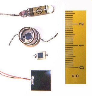
A photodiode is a semiconductor device that converts light into an electrical current. The current is generated when photons are absorbed in the photodiode. Photodiodes may contain optical filters, built-in lenses, and may have large or small surface areas. Photodiodes usually have a slower response time as their surface area increases. The common, traditional solar cell used to generate electric solar power is a large area photodiode.
Complementary metal–oxide–semiconductor (CMOS), also known as complementary-symmetry metal–oxide–semiconductor (COS-MOS), is a type of metal–oxide–semiconductor field-effect transistor (MOSFET) fabrication process that uses complementary and symmetrical pairs of p-type and n-type MOSFETs for logic functions. CMOS technology is used for constructing integrated circuit (IC) chips, including microprocessors, microcontrollers, memory chips, and other digital logic circuits. CMOS technology is also used for analog circuits such as image sensors, data converters, RF circuits, and highly integrated transceivers for many types of communication.

EEPROM (also E2PROM) stands for electrically erasable programmable read-only memory and is a type of non-volatile memory used in computers, integrated in microcontrollers for smart cards and remote keyless systems, and other electronic devices to store relatively small amounts of data but allowing individual bytes to be erased and reprogrammed.

Digital microfluidics (DMF) is another platform for lab-on-a-chip systems that is based upon the manipulation of microdroplets. Droplets are dispensed, moved, stored, mixed, reacted, or analyzed on a platform with a set of insulated electrodes. Digital microfluidics can be used together with analytical analysis procedures such as mass spectrometry, colorimetry, electrochemical, and electrochemiluminescense.
A lab-on-a-chip (LOC) is a device that integrates one or several laboratory functions on a single integrated circuit of only millimeters to a few square centimeters to achieve automation and high-throughput screening. LOCs can handle extremely small fluid volumes down to less than pico-liters. Lab-on-a-chip devices are a subset of microelectromechanical systems (MEMS) devices and sometimes called "micro total analysis systems" (µTAS). LOCs may use microfluidics, the physics, manipulation and study of minute amounts of fluids. However, strictly regarded "lab-on-a-chip" indicates generally the scaling of single or multiple lab processes down to chip-format, whereas "µTAS" is dedicated to the integration of the total sequence of lab processes to perform chemical analysis. The term "lab-on-a-chip" was introduced when it turned out that µTAS technologies were applicable for more than only analysis purposes.

An ion-sensitive field-effect transistor (ISFET) is a field-effect transistor used for measuring ion concentrations in solution; when the ion concentration (such as H+, see pH scale) changes, the current through the transistor will change accordingly. Here, the solution is used as the gate electrode. A voltage between substrate and oxide surfaces arises due to an ion sheath. It is a special type of MOSFET (metal-oxide-semiconductor field-effect transistor), and shares the same basic structure, but with the metal gate replaced by an ion-sensitive membrane, electrolyte solution and reference electrode. Invented in 1970, the ISFET was the first biosensor FET (BioFET).

Microfabrication is the process of fabricating miniature structures of micrometre scales and smaller. Historically, the earliest microfabrication processes were used for integrated circuit fabrication, also known as "semiconductor manufacturing" or "semiconductor device fabrication". In the last two decades microelectromechanical systems (MEMS), microsystems, micromachines and their subfields, microfluidics/lab-on-a-chip, optical MEMS, RF MEMS, PowerMEMS, BioMEMS and their extension into nanoscale have re-used, adapted or extended microfabrication methods. Flat-panel displays and solar cells are also using similar techniques.
The piezoresistive effect is a change in the electrical resistivity of a semiconductor or metal when mechanical strain is applied. In contrast to the piezoelectric effect, the piezoresistive effect causes a change only in electrical resistance, not in electric potential.

An active-pixel sensor (APS) is an image sensor where each pixel sensor unit cell has a photodetector and one or more active transistors. In a metal–oxide–semiconductor (MOS) active-pixel sensor, MOS field-effect transistors (MOSFETs) are used as amplifiers. There are different types of APS, including the early NMOS APS and the much more common complementary MOS (CMOS) APS, also known as the CMOS sensor, which is widely used in digital camera technologies such as cell phone cameras, web cameras, most modern digital pocket cameras, most digital single-lens reflex cameras (DSLRs), and mirrorless interchangeable-lens cameras (MILCs). CMOS sensors emerged as an alternative to charge-coupled device (CCD) image sensors and eventually outsold them by the mid-2000s.
Deep-sub-voltage nanoelectronics are integrated circuits (ICs) operating near theoretical limits of energy consumption per unit of processing. These devices are intended to address the needs of applications such as wireless sensor networks which have dramatically different requirements from traditional electronics. For example, for microprocessors where performance is primary metric of interest, but for some new devices, energy per instruction may be a more sensible metric.

Micropumps are devices that can control and manipulate small fluid volumes. Although any kind of small pump is often referred to as micropump, a more accurate definition restricts this term to pumps with functional dimensions in the micrometer range. Such pumps are of special interest in microfluidic research, and have become available for industrial product integration in recent years. Their miniaturized overall size, potential cost and improved dosing accuracy compared to existing miniature pumps fuel the growing interest for this innovative kind of pump.
Magnetomyography (MMG) is a technique for mapping muscle activity by recording magnetic fields produced by electrical currents occurring naturally in the muscles, using arrays of SQUIDs. It has a better capability than electromyography for detecting slow or direct currents. The magnitude of the MMG signal is in the scale of pico (10−12) to femto (10−15) Tesla (T). Miniaturizing MMG offers a prospect to modernize the bulky SQUID to wearable miniaturized magnetic sensors.
Microelectromechanical system oscillators are timing devices that generate highly stable reference frequencies, which can measure time. These reference frequencies may be used to sequence electronic systems, manage data transfer, define radio frequencies, and measure elapsed time. The core technologies used in MEMS oscillators have been in development since the mid-1960s, but have only been sufficiently advanced for commercial applications since 2006. MEMS oscillators incorporate MEMS resonators, which are microelectromechanical structures that define stable frequencies. MEMS clock generators are MEMS timing devices with multiple outputs for systems that need more than a single reference frequency. MEMS oscillators are a valid alternative to older, more established quartz crystal oscillators, offering better resilience against vibration and mechanical shock, and reliability with respect to temperature variation.
A nanoelectromechanical (NEM) relay is an electrically actuatedswitch that is built on the nanometer scale using semiconductor fabrication techniques. They are designed to operate in replacement, or in conjunction, with traditional semiconductor logic. While the mechanical nature of NEM relays makes them switch much slower than solid-state relays, they have many advantageous properties, such as zero current leakage and low power consumption, which make them potentially useful in next generation computing.
RF CMOS is a metal–oxide–semiconductor (MOS) integrated circuit (IC) technology that integrates radio-frequency (RF), analog and digital electronics on a mixed-signal CMOS RF circuit chip. It is widely used in modern wireless telecommunications, such as cellular networks, Bluetooth, Wi-Fi, GPS receivers, broadcasting, vehicular communication systems, and the radio transceivers in all modern mobile phones and wireless networking devices. RF CMOS technology was pioneered by Pakistani engineer Asad Ali Abidi at UCLA during the late 1980s to early 1990s, and helped bring about the wireless revolution with the introduction of digital signal processing in wireless communications. The development and design of RF CMOS devices was enabled by van der Ziel's FET RF noise model. It was published in the early 1960s and remained largely forgotten until the 1990s.
Orly Yadid-Pecht is a Professor of Electrical and Computer Engineering and Alberta Innovates Technology Futures Strategic Chair of Integrated Intelligent Sensors at the University of Calgary. She develops CMOS based imaging devices for biomedical sensing. She is a Fellow of the Institute of Electrical and Electronics Engineers, SPIE and American Institute for Medical and Biological Engineering. She is an ASTech Award Winner for Technology. Yadid-Pecht holds several patents for new technologies, including sensors, health monitoring devices and drug delivery systems.
The metal–oxide–semiconductor field-effect transistor (MOSFET, MOS-FET, or MOS FET), also known as the metal–oxide–silicon transistor (MOS transistor, or MOS), is a type of insulated-gate field-effect transistor (IGFET) that is fabricated by the controlled oxidation of a semiconductor, typically silicon. The voltage of the covered gate determines the electrical conductivity of the device; this ability to change conductivity with the amount of applied voltage can be used for amplifying or switching electronic signals. The MOSFET was invented by Egyptian engineer Mohamed M. Atalla and Korean engineer Dawon Kahng at Bell Labs in 1959. It is the basic building block of modern electronics, and the most frequently manufactured device in history, with an estimated total of 13 sextillion (1.3 × 10²²) MOSFETs manufactured between 1960 and 2018.
References
- ↑ Zhirnov, Victor; Cavin, Ralph (2008). "Morphic Architectures: Atomic-Level Limits". MRS Online Proceedings Library Archive. 1067. doi:10.1557/PROC-1067-B01-02. ISSN 1946-4274.
- ↑ Cavin, R.; Hutchby, J. A.; Zhirnov, V.; Brewer, J. E.; Bourianoff, G. (2008-05-01). "Emerging Research Architectures". Computer. 41 (5): 33–37. doi:10.1109/MC.2008.155. ISSN 0018-9162. S2CID 3191051.
- ↑ Wise, Kensall D. (2007-05-01). "Integrated sensors, MEMS, and microsystems: Reflections on a fantastic voyage". Sensors and Actuators A: Physical. 136 (1): 39–50. doi:10.1016/j.sna.2007.02.013. ISSN 0924-4247.
- ↑ Rabaey, J.; Ammer, J.; Otis, B.; Burghardt, F.; Chee, Y.H.; Pletcher, N.; Sheets, M.; Qin, H. (2006-07-01). "Ultra-low-power design – The roadmap to disappearing electronics and ambient intelligence". IEEE Circuits and Devices Magazine. 22 (4): 23–29. CiteSeerX 10.1.1.63.6596 . doi:10.1109/MCD.2006.1708372. S2CID 390484.
- ↑ Cooper, Jon M.; Cumming, David R. S.; Reid, Stuart W. J.; Wang, Lei; Johannessen, Erik A. (2006-12-20). "Implementation of radiotelemetry in a lab-in-a-pill format". Lab on a Chip. 6 (1): 39–45. doi:10.1039/B507312J. ISSN 1473-0189. PMID 16372067.
- ↑ Cook, B. W.; Lanzisera, S.; Pister, K. S. J. (2006-06-01). "SoC Issues for RF Smart Dust". Proceedings of the IEEE. 94 (6): 1177–1196. doi:10.1109/JPROC.2006.873620. ISSN 0018-9219. S2CID 16089712.