
Nanocrystalline silicon (nc-Si), sometimes also known as microcrystalline silicon (μc-Si), is a form of porous silicon. It is an allotropic form of silicon with paracrystalline structure—is similar to amorphous silicon (a-Si), in that it has an amorphous phase. Where they differ, however, is that nc-Si has small grains of crystalline silicon within the amorphous phase. This is in contrast to polycrystalline silicon (poly-Si) which consists solely of crystalline silicon grains, separated by grain boundaries. The difference comes solely from the grain size of the crystalline grains. Most materials with grains in the micrometre range are actually fine-grained polysilicon, so nanocrystalline silicon is a better term. The term Nanocrystalline silicon refers to a range of materials around the transition region from amorphous to microcrystalline phase in the silicon thin film. The crystalline volume fraction is another criterion to describe the materials in this transition zone.
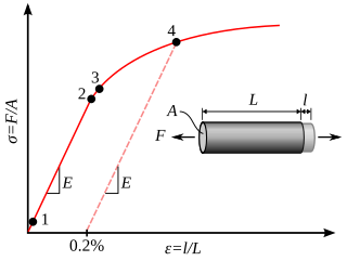
In physics and materials science, plasticity, also known as plastic deformation, is the ability of a solid material to undergo permanent deformation, a non-reversible change of shape in response to applied forces. For example, a solid piece of metal being bent or pounded into a new shape displays plasticity as permanent changes occur within the material itself. In engineering, the transition from elastic behavior to plastic behavior is known as yielding.

An amorphous metal is a solid metallic material, usually an alloy, with disordered atomic-scale structure. Most metals are crystalline in their solid state, which means they have a highly ordered arrangement of atoms. Amorphous metals are non-crystalline, and have a glass-like structure. But unlike common glasses, such as window glass, which are typically electrical insulators, amorphous metals have good electrical conductivity and they also display superconductivity at low temperatures.

A crystallite is a small or even microscopic crystal which forms, for example, during the cooling of many materials. The orientation of crystallites can be random with no preferred direction, called random texture, or directed, possibly due to growth and processing conditions. Fiber texture is an example of the latter. Crystallites are also referred to as grains. The areas where crystallites meet are known as grain boundaries. Polycrystalline materials, or polycrystals, are solids that are composed of many crystallites of varying size and orientation.
Liquidmetal and Vitreloy are commercial names of a series of amorphous metal alloys developed by a California Institute of Technology (Caltech) research team and marketed by Liquidmetal Technologies. Liquidmetal alloys combine a number of desirable material features, including high tensile strength, excellent corrosion resistance, very high coefficient of restitution and excellent anti-wearing characteristics, while also being able to be heat-formed in processes similar to thermoplastics. Despite the name, they are not liquid at room temperature.
A nanostructure is a structure of intermediate size between microscopic and molecular structures. Nanostructural detail is microstructure at nanoscale.
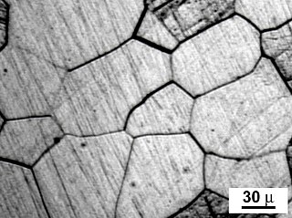
A grain boundary is the interface between two grains, or crystallites, in a polycrystalline material. Grain boundaries are 2D defects in the crystal structure, and tend to decrease the electrical and thermal conductivity of the material. Most grain boundaries are preferred sites for the onset of corrosion and for the precipitation of new phases from the solid. They are also important to many of the mechanisms of creep. On the other hand, grain boundaries disrupt the motion of dislocations through a material, so reducing crystallite size is a common way to improve mechanical strength, as described by the Hall–Petch relationship. The study of grain boundaries and their effects on the mechanical, electrical and other properties of materials forms an important topic in materials science.

A superalloy, or high-performance alloy, is an alloy with the ability to operate at a high fraction of its melting point. Several key characteristics of a superalloy are excellent mechanical strength, resistance to thermal creep deformation, good surface stability, and resistance to corrosion or oxidation.

Heusler compounds are magnetic intermetallics with face-centered cubic crystal structure and a composition of XYZ (half-Heuslers) or X2YZ (full-Heuslers), where X and Y are transition metals and Z is in the p-block. Many of these compounds exhibit properties relevant to spintronics, such as magnetoresistance, variations of the Hall effect, ferro-, antiferro-, and ferrimagnetism, half- and semimetallicity, semiconductivity with spin filter ability, superconductivity, and topological band structure. Their magnetism results from a double-exchange mechanism between neighboring magnetic ions. Manganese, which sits at the body centers of the cubic structure, was the magnetic ion in the first Heusler compound discovered. (See the Bethe–Slater curve for details of why this happens.)
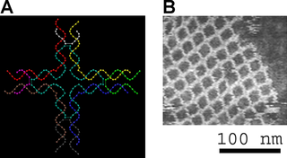
Nanocomposite is a multiphase solid material where one of the phases has one, two or three dimensions of less than 100 nanometers (nm) or structures having nano-scale repeat distances between the different phases that make up the material.
A nanocrystalline (NC) material is a polycrystalline material with a crystallite size of only a few nanometers. These materials fill the gap between amorphous materials without any long range order and conventional coarse-grained materials. Definitions vary, but nanocrystalline material is commonly defined as a crystallite (grain) size below 100 nm. Grain sizes from 100–500 nm are typically considered "ultrafine" grains.
Pseudoelasticity, sometimes called superelasticity, is an elastic (reversible) response to an applied stress, caused by a phase transformation between the austenitic and martensitic phases of a crystal. It is exhibited in shape-memory alloys.
High-power impulse magnetron sputtering is a method for physical vapor deposition of thin films which is based on magnetron sputter deposition. HIPIMS utilises extremely high power densities of the order of kW⋅cm−2 in short pulses (impulses) of tens of microseconds at low duty cycle of < 10%. Distinguishing features of HIPIMS are a high degree of ionisation of the sputtered metal and a high rate of molecular gas dissociation which result in high density of deposited films. The ionization and dissociation degree increase according to the peak cathode power. The limit is determined by the transition of the discharge from glow to arc phase. The peak power and the duty cycle are selected so as to maintain an average cathode power similar to conventional sputtering (1–10 W⋅cm−2).

Grain-boundary strengthening is a method of strengthening materials by changing their average crystallite (grain) size. It is based on the observation that grain boundaries are insurmountable borders for dislocations and that the number of dislocations within a grain have an effect on how stress builds up in the adjacent grain, which will eventually activate dislocation sources and thus enabling deformation in the neighbouring grain, too. So, by changing grain size one can influence the number of dislocations piled up at the grain boundary and yield strength. For example, heat treatment after plastic deformation and changing the rate of solidification are ways to alter grain size.
Severe plastic deformation (SPD) is a generic term describing a group of metalworking techniques involving very large strains typically involving a complex stress state or high shear, resulting in a high defect density and equiaxed "ultrafine" grain (UFG) size or nanocrystalline (NC) structure.
Reactive bonding describes a wafer bonding procedure using highly reactive nanoscale multilayer systems as an intermediate layer between the bonding substrates. The multilayer system consists of two alternating different thin metallic films. The self-propagating exothermic reaction within the multilayer system contributes the local heat to bond the solder films. Based on the limited temperature the substrate material is exposed, temperature-sensitive components and materials with different CTEs, i.e. metals, polymers and ceramics, can be used without thermal damage.
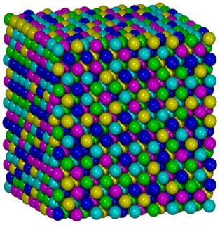
High-entropy alloys (HEAs) are alloys that are formed by mixing equal or relatively large proportions of (usually) five or more elements. Prior to the synthesis of these substances, typical metal alloys comprised one or two major components with smaller amounts of other elements. For example, additional elements can be added to iron to improve its properties, thereby creating an iron based alloy, but typically in fairly low proportions, such as the proportions of carbon, manganese, and the like in various steels. Hence, high entropy alloys are a novel class of materials. The term “high-entropy alloys” was coined because the entropy increase of mixing is substantially higher when there is a larger number of elements in the mix, and their proportions are more nearly equal.
Dislocation avalanches are rapid discreet events during plastic deformation, in which defects are reorganized collectively. This intermittent flow behavior has been observed in microcrystals, whereas macroscopic plasticity appears as a smooth process. Intermittent plastic flow has been observed in several different systems. In AlMg Alloys, interaction between solute and dislocations can cause sudden jump during dynamic strain aging. In metallic glass, it can be observed via shear banding with stress localization; and single crystal plasticity, it shows up as slip burst. However, analysis of the events with orders-magnitude difference in sizes with different crystallographic structure reveals power-law scaling between the number of events and their magnitude, or scale-free flow.
Two dimensional hexagonal boron nitride is a material of comparable structure to graphene with potential applications in e.g. photonics., fuel cells and as a substrate for two-dimensional heterostructures. 2D h-BN is isostructural to graphene, but where graphene is conductive, 2D h-BN is a wide-gap insulator.
Electron channelling contrast imaging (ECCI) is a scanning electron microscope (SEM) diffraction technique used in the study of defects in materials. These can be dislocations or stacking faults that are close to the surface of the sample, low angle grain boundaries or atomic steps. Unlike the use of transmission electron microscopy (TEM) for the investigation of dislocations, the ECCI approach has been called a rapid and non-destructive characterisation technique
