
MEMS is the technology of microscopic devices incorporating both electronic and moving parts. MEMS are made up of components between 1 and 100 micrometres in size, and MEMS devices generally range in size from 20 micrometres to a millimetre, although components arranged in arrays can be more than 1000 mm2. They usually consist of a central unit that processes data and several components that interact with the surroundings.

A digital camera, also called a digicam, is a camera that captures photographs in digital memory. Most cameras produced today are digital, largely replacing those that capture images on photographic film or film stock. Digital cameras are now widely incorporated into mobile devices like smartphones with the same or more capabilities and features of dedicated cameras. High-end, high-definition dedicated cameras are still commonly used by professionals and those who desire to take higher-quality photographs.

A smartphone, often simply called a phone, is a mobile device that combines the functionality of a traditional mobile phone with advanced computing capabilities. It typically has a touchscreen interface, allowing users to access a wide range of applications and services, such as web browsing, email, and social media, as well as multimedia playback and streaming. Smartphones have built-in cameras, GPS navigation, and support for various communication methods, including voice calls, text messaging, and internet-based messaging apps.

A camera phone is a mobile phone that is able to capture photographs and often record video using one or more built-in digital cameras. It can also send the resulting image wirelessly and conveniently. The first commercial phone with a color camera was the Kyocera Visual Phone VP-210, released in Japan in May 1999.

A handheld projector is an image projector in a handheld device. It was developed as a computer display device for compact portable devices such as mobile phones, personal digital assistants, and digital cameras, which have sufficient storage capacity to handle presentation materials but are too small to accommodate a display screen that an audience can see easily. Handheld projectors involve miniaturized hardware, and software that can project digital images onto a nearby viewing surface.
Archos is a French multinational electronics company that was established in 1988 by Henri Crohas. Archos manufactures tablets, smartphones, portable media players and portable data storage devices. The name is an anagram of Crohas' last name. Also, in Greek (-αρχος), it's a suffix used in nouns indicating a person with power. The company's slogan has been updated from "Think Smaller" to "On The Go", and the current "Entertainment your way".
OmniVision Technologies Inc. is an American subsidiary of Chinese semiconductor device and mixed-signal integrated circuit design house Will Semiconductor. The company designs and develops digital imaging products for use in mobile phones, laptops, netbooks webcams, security, entertainment, automotive and medical imaging systems. Headquartered in Santa Clara, California, OmniVision Technologies has offices in the US, Western Europe and Asia.
A three-dimensional integrated circuit is a MOS integrated circuit (IC) manufactured by stacking as many as 16 or more ICs and interconnecting them vertically using, for instance, through-silicon vias (TSVs) or Cu-Cu connections, so that they behave as a single device to achieve performance improvements at reduced power and smaller footprint than conventional two dimensional processes. The 3D IC is one of several 3D integration schemes that exploit the z-direction to achieve electrical performance benefits in microelectronics and nanoelectronics.

A microlens is a small lens, generally with a diameter less than a millimetre (mm) and often as small as 10 micrometres (μm). The small sizes of the lenses means that a simple design can give good optical quality but sometimes unwanted effects arise due to optical diffraction at the small features. A typical microlens may be a single element with one plane surface and one spherical convex surface to refract the light. Because micro-lenses are so small, the substrate that supports them is usually thicker than the lens and this has to be taken into account in the design. More sophisticated lenses may use aspherical surfaces and others may use several layers of optical material to achieve their design performance.

Wafer-level packaging (WLP) is a process in integrated circuit manufacturing where packaging components are attached to an integrated circuit (IC) before the wafer – on which the IC is fabricated – is diced. In WLP, the top and bottom layers of the packaging and the solder bumps are attached to the integrated circuits while they are still in the wafer. This process differs from a conventional process, in which the wafer is sliced into individual circuits (dice) before the packaging components are attached.
Himax Technologies, Inc. is a fabless semiconductor manufacturer headquartered in Tainan City, Taiwan founded on 12 June 2001. The company is publicly traded and listed on the Nasdaq Stock Market under the symbol HIMX. Himax Technologies Limited functions as a holding under the Cayman Islands Companies Law.
Suss Microtec is a supplier of equipment and process solutions for the semiconductor, nano and microsystems technology and related markets with headquarters in Garching near Munich.

A back-illuminated sensor, also known as backside illumination (BI) sensor, is a type of digital image sensor that uses a novel arrangement of the imaging elements to increase the amount of light captured and thereby improve low-light performance.

Nokia PureView is the branding of a combination of technologies used in cameras of Nokia-branded smartphones and previously, in phones by Microsoft Mobile. PureView was first introduced with the Nokia 808 PureView.
AuthenTec, Inc. was a semiconductor, computer security, mobile security, identity management, biometrics, and touch control solutions company based in Melbourne, Florida. Founded in 1998 after being spun off from Harris Semiconductor, AuthenTec provided mobile security software licenses to mobile manufacturing companies, and biometrics sensor technology, such as fingerprint sensors and NFC technology to mobile and computer manufacturers. On 27 July 2012, AuthenTec was acquired by Apple Inc. for $356 million.

Advanced Semiconductor Engineering, Inc., previously known as ASE Group, is a leading provider of independent semiconductor packaging and test manufacturing services, with its headquarters in Kaohsiung, Taiwan.

Fan-out wafer-level packaging is an integrated circuit packaging technology, and an enhancement of standard wafer-level packaging (WLP) solutions. Fan-out packaging is seen as a low cost advanced packaging alternative to packages that use silicon interposers, such as those seen in 2.5D and 3D packages.
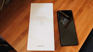
The Sony Xperia 1 II is an Android smartphone manufactured by Sony Mobile. Part of Sony's Xperia series, the phone was announced along with the mid-range Xperia 10 II on February 24, 2020. Key upgrades over its predecessor, the Xperia 1, include support for 5G connectivity and Qi wireless charging, and a triple-lens camera which incorporates ZEISS-branded lenses with T✻ (T-Star) anti-reflective coating as well as technology brought over from Sony's Alpha camera lineup.

The Samsung Galaxy A41 is a mid-range Android smartphone developed by Samsung Electronics as part of their 2020 A-series smartphone lineup. It was announced on 18 March 2020, and first released in Europe on 22 May 2020 as the successor to the Galaxy A40. The phone comes preinstalled with Android 10 and Samsung’s custom One UI 2.1 software overlay, but was upgraded to Android 12 and One UI 4.1 with the updates starting on 29 September 2022.
The Sony Xperia PRO is an Android smartphone manufactured by Sony Mobile. It is exclusive to the United States, Japan, and Europe, and is intended as a phone for video professionals, offering HDMI input and mmWave 5G connectivity.