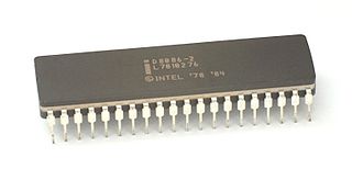
x86 is a family of complex instruction set computer (CISC) instruction set architectures initially developed by Intel based on the Intel 8086 microprocessor and its 8088 variant. The 8086 was introduced in 1978 as a fully 16-bit extension of Intel's 8-bit 8080 microprocessor, with memory segmentation as a solution for addressing more memory than can be covered by a plain 16-bit address. The term "x86" came into being because the names of several successors to Intel's 8086 processor end in "86", including the 80186, 80286, 80386 and 80486 processors. Colloquially, their names were "186", "286", "386" and "486".

A memory management unit (MMU), sometimes called paged memory management unit (PMMU), is a computer hardware unit that examines all memory references on the memory bus, translating these requests, known as virtual memory addresses, into physical addresses in main memory.

x86-64 is a CISC type processor, a 64-bit version of the x86 instruction set, first announced in 1999. It introduced two new modes of operation, 64-bit mode and compatibility mode, along with a new 4-level paging mode.
In computing, Physical Address Extension (PAE), sometimes referred to as Page Address Extension, is a memory management feature for the x86 architecture. PAE was first introduced by Intel in the Pentium Pro, and later by AMD in the Athlon processor. It defines a page table hierarchy of three levels (instead of two), with table entries of 64 bits each instead of 32, allowing these CPUs to directly access a physical address space larger than 4 gigabytes (232 bytes).
A translation lookaside buffer (TLB) is a memory cache that stores the recent translations of virtual memory to physical memory. It is used to reduce the time taken to access a user memory location. It can be called an address-translation cache. It is a part of the chip's memory-management unit (MMU). A TLB may reside between the CPU and the CPU cache, between CPU cache and the main memory or between the different levels of the multi-level cache. The majority of desktop, laptop, and server processors include one or more TLBs in the memory-management hardware, and it is nearly always present in any processor that utilizes paged or segmented virtual memory.
The x86 instruction set refers to the set of instructions that x86-compatible microprocessors support. The instructions are usually part of an executable program, often stored as a computer file and executed on the processor.
In the 80386 microprocessor and later, virtual 8086 mode allows the execution of real mode applications that are incapable of running directly in protected mode while the processor is running a protected mode operating system. It is a hardware virtualization technique that allowed multiple 8086 processors to be emulated by the 386 chip. It emerged from the painful experiences with the 80286 protected mode, which by itself was not suitable to run concurrent real-mode applications well. John Crawford developed the Virtual Mode bit at the register set, paving the way to this environment.
The NX bit (no-execute) is a technology used in CPUs to segregate areas of a virtual address space to store either data or processor instructions. An operating system with support for the NX bit may mark certain areas of an address space as non-executable. The processor will then refuse to execute any code residing in these areas of the address space. The general technique, known as executable space protection, also called Write XOR Execute, is used to prevent certain types of malicious software from taking over computers by inserting their code into another program's data storage area and running their own code from within this section; one class of such attacks is known as the buffer overflow attack.
A CPU cache is a hardware cache used by the central processing unit (CPU) of a computer to reduce the average cost to access data from the main memory. A cache is a smaller, faster memory, located closer to a processor core, which stores copies of the data from frequently used main memory locations. Most CPUs have a hierarchy of multiple cache levels, with different instruction-specific and data-specific caches at level 1. The cache memory is typically implemented with static random-access memory (SRAM), in modern CPUs by far the largest part of them by chip area, but SRAM is not always used for all levels, or even any level, sometimes some latter or all levels are implemented with eDRAM.
Memory segmentation is an operating system memory management technique of dividing a computer's primary memory into segments or sections. In a computer system using segmentation, a reference to a memory location includes a value that identifies a segment and an offset within that segment. Segments or sections are also used in object files of compiled programs when they are linked together into a program image and when the image is loaded into memory.
The Intel Core microarchitecture is a multi-core processor microarchitecture launched by Intel in mid-2006. It is a major evolution over the Yonah, the previous iteration of the P6 microarchitecture series which started in 1995 with Pentium Pro. It also replaced the NetBurst microarchitecture, which suffered from high power consumption and heat intensity due to an inefficient pipeline designed for high clock rate. In early 2004 the new version of NetBurst (Prescott) needed very high power to reach the clocks it needed for competitive performance, making it unsuitable for the shift to dual/multi-core CPUs. On May 7, 2004 Intel confirmed the cancellation of the next NetBurst, Tejas and Jayhawk. Intel had been developing Merom, the 64-bit evolution of the Pentium M, since 2001, and decided to expand it to all market segments, replacing NetBurst in desktop computers and servers. It inherited from Pentium M the choice of a short and efficient pipeline, delivering superior performance despite not reaching the high clocks of NetBurst.
In the x86-64 computer architecture, long mode is the mode where a 64-bit operating system can access 64-bit instructions and registers. 64-bit programs are run in a sub-mode called 64-bit mode, while 32-bit programs and 16-bit protected mode programs are executed in a sub-mode called compatibility mode. Real mode or virtual 8086 mode programs cannot be natively run in long mode.
In the x86 architecture, the CPUID instruction is a processor supplementary instruction allowing software to discover details of the processor. It was introduced by Intel in 1993 with the launch of the Pentium and SL-enhanced 486 processors.

Pentium is a semi-discontinued series of x86 architecture-compatible microprocessors produced by Intel. The original Pentium was first released on March 22, 1993. The name "Pentium" is originally derived from the Greek word pente (πεντε), meaning "five", a reference to the prior numeric naming convention of Intel's 80x86 processors (8086–80486), with the Latin ending -ium since the processor would otherwise have been named 80586 using that convention.
A control register is a processor register that changes or controls the general behavior of a CPU or other digital device. Common tasks performed by control registers include interrupt control, switching the addressing mode, paging control, and coprocessor control.
On the x86 architecture, a debug register is a register used by a processor for program debugging. There are six debug registers, named DR0...DR7, with DR4 and DR5 as obsolete synonyms for DR6 and DR7. The debug registers allow programmers to selectively enable various debug conditions associated with a set of four debug addresses. Two of these registers are used to control debug features. These registers are accessed by variants of the MOV instruction. A debug register may be either the source operand or destination operand. The debug registers are privileged resources; the MOV instructions that access them can only be executed at privilege level zero. An attempt to read or write the debug registers when executing at any other privilege level causes a general protection fault.
A page, memory page, or virtual page is a fixed-length contiguous block of virtual memory, described by a single entry in a page table of an operating system. It is the smallest unit of data for memory management in an operating system that uses virtual memory. Similarly, a page frame is the smallest fixed-length contiguous block of physical memory into which memory pages are mapped by the operating system.
In computing, PSE-36 refers to a feature of x86 processors that extends the physical memory addressing capabilities from 32 bits to 36 bits, allowing addressing to up to 64 GB of memory. Compared to the Physical Address Extension (PAE) method, PSE-36 is a simpler alternative to addressing more than 4 GB of memory. It uses the Page Size Extension (PSE) mode and a modified page directory table to map 4 MB pages into a 64 GB physical address space. PSE-36's downside is that, unlike PAE, it doesn't have 4-KB page granularity above the 4 GB mark.
In computing, the term 3 GB barrier refers to a limitation of some 32-bit operating systems running on x86 microprocessors. It prevents the operating systems from using all of 4 GiB (4 × 10243 bytes) of main memory. The exact barrier varies by motherboard and I/O device configuration, particularly the size of video RAM; it may be in the range of 2.75 GB to 3.5 GB. The barrier is not present with a 64-bit processor and 64-bit operating system, or with certain x86 hardware and an operating system such as Linux or certain versions of Windows Server and macOS that allow use of Physical Address Extension (PAE) mode on x86 to access more than 4 GiB of RAM.

Intel 5-level paging, referred to simply as 5-level paging in Intel documents, is a processor extension for the x86-64 line of processors. It extends the size of virtual addresses from 48 bits to 57 bits, increasing the addressable virtual memory from 256 TB to 128 PB. The extension was first implemented in the Ice Lake processors, and the 4.14 Linux kernel adds support for it. Windows 10 and 11 with server versions also support this extension in their latest updates, where it is provided by a separate kernel of the system called ntkrla57.exe.

