Related Research Articles

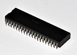
An integrated circuit or monolithic integrated circuit is a set of electronic circuits on one small flat piece of semiconductor material, usually silicon. Large numbers of tiny MOSFETs integrate into a small chip. This results in circuits that are orders of magnitude smaller, faster, and less expensive than those constructed of discrete electronic components. The IC's mass production capability, reliability, and building-block approach to integrated circuit design has ensured the rapid adoption of standardized ICs in place of designs using discrete transistors. ICs are now used in virtually all electronic equipment and have revolutionized the world of electronics. Computers, mobile phones and other home appliances are now inextricable parts of the structure of modern societies, made possible by the small size and low cost of ICs such as modern computer processors and microcontrollers.
In electronics and photonics design, tape-out or tapeout is the final result of the design process for integrated circuits or printed circuit boards before they are sent for manufacturing. The tapeout is specifically the point at which the graphic for the photomask of the circuit is sent to the fabrication facility.

An application-specific integrated circuit is an integrated circuit (IC) chip customized for a particular use, rather than intended for general-purpose use. For example, a chip designed to run in a digital voice recorder or a high-efficiency video codec is an ASIC. Application-specific standard product (ASSP) chips are intermediate between ASICs and industry standard integrated circuits like the 7400 series or the 4000 series. ASIC chips are typically fabricated using metal-oxide-semiconductor (MOS) technology, as MOS integrated circuit chips.
Electronic design automation (EDA), also referred to as electronic computer-aided design (ECAD), is a category of software tools for designing electronic systems such as integrated circuits and printed circuit boards. The tools work together in a design flow that chip designers use to design and analyze entire semiconductor chips. Since a modern semiconductor chip can have billions of components, EDA tools are essential for their design; this article in particular describes EDA specifically with respect to integrated circuits (ICs).

Synopsys is an American electronic design automation company that focuses on silicon design and verification, silicon intellectual property and software security and quality. Products include logic synthesis, behavioral synthesis, place and route, static timing analysis, formal verification, hardware description language simulators, and transistor-level circuit simulation. The simulators include development and debugging environments that assist in the design of the logic for chips and computer systems. In recent years, Synopsys has expanded its products and services to include application security testing. Their technology is present in self-driving cars, artificial intelligence, and internet of things consumer products.

A gate array is an approach to the design and manufacture of application-specific integrated circuits (ASICs) using a prefabricated chip with components that are later interconnected into logic devices according to a custom order by adding metal interconnect layers in the factory. It was popular during upheaval in semiconductor industry in 80s and its usage declined by end of 90s.

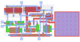
Integrated circuit layout, also known IC layout, IC mask layout, or mask design, is the representation of an integrated circuit in terms of planar geometric shapes which correspond to the patterns of metal, oxide, or semiconductor layers that make up the components of the integrated circuit. Originally the overall process was called tapeout as historically early ICs used graphical black crepe tape on mylar media for photo imaging.

Silvaco Inc. develops and markets electronic design automation (EDA) and technology CAD (TCAD) software and semiconductor design IP (SIP). The company is headquartered in Santa Clara, California, and has a global presence with offices located in North America, Europe, and throughout Asia. Since its founding in 1984, Silvaco has grown to become a large privately held EDA company. The company has been known by at least two other names: Silvaco International, and Silvaco Data Systems.
GDSII stream format (GDSII), is a binary database file format which is the de facto industry standard for Electronic Design Automation data exchange of integrated circuit or IC layout artwork. It is a binary file format representing planar geometric shapes, text labels, and other information about the layout in hierarchical form. The data can be used to reconstruct all or part of the artwork to be used in sharing layouts, transferring artwork between different tools, or creating photomasks.
In electronics engineering, a design rule is a geometric constraint imposed on circuit board, semiconductor device, and integrated circuit (IC) designers to ensure their designs function properly, reliably, and can be produced with acceptable yield. Design rules for production are developed by process engineers based on the capability of their processes to realize design intent. Electronic design automation is used extensively to ensure that designers do not violate design rules; a process called design rule checking (DRC). DRC is a major step during physical verification signoff on the design, which also involves LVS checks, XOR checks, ERC, and antenna checks. The importance of design rules and DRC is greatest for ICs, which have micro- or nano-scale geometries; for advanced processes, some fabs also insist upon the use of more restricted rules to improve yield.
In electronic design, a semiconductor intellectual property core, IP core, or IP block is a reusable unit of logic, cell, or integrated circuit layout design that is the intellectual property of one party. IP cores can be licensed to another party or owned and used by a single party. The term comes from the licensing of the patent or source code copyright that exists in the design. Designers of application-specific integrated circuits (ASIC) and systems of field-programmable gate array (FPGA) logic can use IP cores as building blocks.
In semiconductor design, standard cell methodology is a method of designing application-specific integrated circuits (ASICs) with mostly digital-logic features. Standard cell methodology is an example of design abstraction, whereby a low-level very-large-scale integration (VLSI) layout is encapsulated into an abstract logic representation.

Integrated circuit design, or IC design, is a sub-field of electronics engineering, encompassing the particular logic and circuit design techniques required to design integrated circuits, or ICs. ICs consist of miniaturized electronic components built into an electrical network on a monolithic semiconductor substrate by photolithography.
Resolution enhancement technologies are methods used to modify the photomasks in the lithographic processes used to make integrated circuits to compensate for limitations in the optical resolution of the projection systems. These processes allow the creation of features well beyond the limit that would normally apply due to the Rayleigh criterion. Modern technologies allow the creation of features on the order of 5 nanometers (nm), far below the normal resolution possible using deep ultraviolet (DUV) light.
An EDA database is a database specialized for the purpose of electronic design automation. These application specific databases are required because general purpose databases have historically not provided enough performance for EDA applications.

Multi-project chip (MPC), and multi-project wafer (MPW) semiconductor manufacturing arrangements allow customers to share mask and microelectronics wafer fabrication cost between several designs or projects.
SmartSpice is a commercial version of SPICE developed by Silvaco. SmartSpice is used to design complex analog circuits, analyze critical nets, characterize cell libraries, and verify analog mixed-signal designs. SmartSpice is compatible with popular analog design flows and foundry-supplied device models. It supports a reduced design space simulation environment. Among its usages in the electronics industry is Dynamic Timing Analysis.

In integrated circuit design, physical design is a step in the standard design cycle which follows after the circuit design. At this step, circuit representations of the components of the design are converted into geometric representations of shapes which, when manufactured in the corresponding layers of materials, will ensure the required functioning of the components. This geometric representation is called integrated circuit layout. This step is usually split into several sub-steps, which include both design and verification and validation of the layout.

Michael Hochberg is an American physicist. He’s authored over 100 peer-reviewed journal articles, has founded several companies, and has been an inventor on over 60 patents. Hochberg's research interests include silicon photonics and large-scale photonic integration. He has worked in a number of application areas, including data communications, biosensing, quantum optics, mid-infrared photonics, optical computing, and machine learning. Much of his work in silicon photonics has been the product of a longstanding series of collaborations with Thomas Baehr-Jones.
In the automated design of integrated circuits, signoff checks is the collective name given to a series of verification steps that the design must pass before it can be taped out. This implies an iterative process involving incremental fixes across the board using one or more check types, and then retesting the design. There are two types of sign-off's: front-end sign-off and back-end sign-off. After back-end sign-off the chip goes to fabrication. After listing out all the features in the specification, the verification engineer will write coverage for those features to identify bugs, and send back the RTL design to the designer. Bugs, or defects, can include issues like missing features, errors in design, etc. When the coverage reaches a maximum% then the verification team will sign it off. By using a methodology like UVM, OVM, or VMM, the verification team develops a reusable environment. Nowadays, UVM is more popular than others.