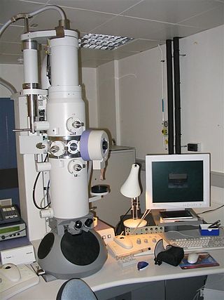
An electron microscope is a microscope that uses a beam of electrons as a source of illumination. They use electron optics that are analogous to the glass lenses of an optical light microscope to control the electron beam, for instance focusing them to produce magnified images or electron diffraction patterns. As the wavelength of an electron can be up to 100,000 times smaller than that of visible light, electron microscopes have a much higher resolution of about 0.1 nm, which compares to about 200 nm for light microscopes. Electron microscope may refer to:

Microscopy is the technical field of using microscopes to view objects and areas of objects that cannot be seen with the naked eye. There are three well-known branches of microscopy: optical, electron, and scanning probe microscopy, along with the emerging field of X-ray microscopy.

A microscope is a laboratory instrument used to examine objects that are too small to be seen by the naked eye. Microscopy is the science of investigating small objects and structures using a microscope. Microscopic means being invisible to the eye unless aided by a microscope.

A scanning electron microscope (SEM) is a type of electron microscope that produces images of a sample by scanning the surface with a focused beam of electrons. The electrons interact with atoms in the sample, producing various signals that contain information about the surface topography and composition of the sample. The electron beam is scanned in a raster scan pattern, and the position of the beam is combined with the intensity of the detected signal to produce an image. In the most common SEM mode, secondary electrons emitted by atoms excited by the electron beam are detected using a secondary electron detector. The number of secondary electrons that can be detected, and thus the signal intensity, depends, among other things, on specimen topography. Some SEMs can achieve resolutions better than 1 nanometer.

Surface science is the study of physical and chemical phenomena that occur at the interface of two phases, including solid–liquid interfaces, solid–gas interfaces, solid–vacuum interfaces, and liquid–gas interfaces. It includes the fields of surface chemistry and surface physics. Some related practical applications are classed as surface engineering. The science encompasses concepts such as heterogeneous catalysis, semiconductor device fabrication, fuel cells, self-assembled monolayers, and adhesives. Surface science is closely related to interface and colloid science. Interfacial chemistry and physics are common subjects for both. The methods are different. In addition, interface and colloid science studies macroscopic phenomena that occur in heterogeneous systems due to peculiarities of interfaces.

Atomic force microscopy (AFM) or scanning force microscopy (SFM) is a very-high-resolution type of scanning probe microscopy (SPM), with demonstrated resolution on the order of fractions of a nanometer, more than 1000 times better than the optical diffraction limit.
Scanning probe microscopy (SPM) is a branch of microscopy that forms images of surfaces using a physical probe that scans the specimen. SPM was founded in 1981, with the invention of the scanning tunneling microscope, an instrument for imaging surfaces at the atomic level. The first successful scanning tunneling microscope experiment was done by Gerd Binnig and Heinrich Rohrer. The key to their success was using a feedback loop to regulate gap distance between the sample and the probe.

Confocal microscopy, most frequently confocal laser scanning microscopy (CLSM) or laser scanning confocal microscopy (LSCM), is an optical imaging technique for increasing optical resolution and contrast of a micrograph by means of using a spatial pinhole to block out-of-focus light in image formation. Capturing multiple two-dimensional images at different depths in a sample enables the reconstruction of three-dimensional structures within an object. This technique is used extensively in the scientific and industrial communities and typical applications are in life sciences, semiconductor inspection and materials science.

Magnetic force microscopy (MFM) is a variety of atomic force microscopy, in which a sharp magnetized tip scans a magnetic sample; the tip-sample magnetic interactions are detected and used to reconstruct the magnetic structure of the sample surface. Many kinds of magnetic interactions are measured by MFM, including magnetic dipole–dipole interaction. MFM scanning often uses non-contact AFM (NC-AFM) mode.
Characterization, when used in materials science, refers to the broad and general process by which a material's structure and properties are probed and measured. It is a fundamental process in the field of materials science, without which no scientific understanding of engineering materials could be ascertained. The scope of the term often differs; some definitions limit the term's use to techniques which study the microscopic structure and properties of materials, while others use the term to refer to any materials analysis process including macroscopic techniques such as mechanical testing, thermal analysis and density calculation. The scale of the structures observed in materials characterization ranges from angstroms, such as in the imaging of individual atoms and chemical bonds, up to centimeters, such as in the imaging of coarse grain structures in metals.

A scanning acoustic microscope (SAM) is a device which uses focused sound to investigate, measure, or image an object. It is commonly used in failure analysis and non-destructive evaluation. It also has applications in biological and medical research. The semiconductor industry has found the SAM useful in detecting voids, cracks, and delaminations within microelectronic packages.

Nanometrology is a subfield of metrology, concerned with the science of measurement at the nanoscale level. Nanometrology has a crucial role in order to produce nanomaterials and devices with a high degree of accuracy and reliability in nanomanufacturing.
Scanning capacitance microscopy (SCM) is a variety of scanning probe microscopy in which a narrow probe electrode is positioned in contact or close proximity of a sample's surface and scanned. SCM characterizes the surface of the sample using information obtained from the change in electrostatic capacitance between the surface and the probe.
Photothermal microspectroscopy (PTMS), alternatively known as photothermal temperature fluctuation (PTTF), is derived from two parent instrumental techniques: infrared spectroscopy and atomic force microscopy (AFM). In one particular type of AFM, known as scanning thermal microscopy (SThM), the imaging probe is a sub-miniature temperature sensor, which may be a thermocouple or a resistance thermometer. This same type of detector is employed in a PTMS instrument, enabling it to provide AFM/SThM images: However, the chief additional use of PTMS is to yield infrared spectra from sample regions below a micrometer, as outlined below.
Acoustic microscopy is microscopy that employs very high or ultra high frequency ultrasound. Acoustic microscopes operate non-destructively and penetrate most solid materials to make visible images of internal features, including defects such as cracks, delaminations and voids.

Scanning thermal microscopy (SThM) is a type of scanning probe microscopy that maps the local temperature and thermal conductivity of an interface. The probe in a scanning thermal microscope is sensitive to local temperatures – providing a nano-scale thermometer. Thermal measurements at the nanometer scale are of both scientific and industrial interest. The technique was invented by Clayton C. Williams and H. Kumar Wickramasinghe in 1986.
Endomicroscopy is a technique for obtaining histology-like images from inside the human body in real-time, a process known as ‘optical biopsy’. It generally refers to fluorescence confocal microscopy, although multi-photon microscopy and optical coherence tomography have also been adapted for endoscopic use. Commercially available clinical and pre-clinical endomicroscopes can achieve a resolution on the order of a micrometre, have a field-of-view of several hundred µm, and are compatible with fluorophores which are excitable using 488 nm laser light. The main clinical applications are currently in imaging of the tumour margins of the brain and gastro-intestinal tract, particularly for the diagnosis and characterisation of Barrett’s Esophagus, pancreatic cysts and colorectal lesions. A number of pre-clinical and transnational applications have been developed for endomicroscopy as it enables researchers to perform live animal imaging. Major pre-clinical applications are in gastro-intestinal tract, toumour margin detection, uterine complications, ischaemia, live imaging of cartilage and tendon and organoid imaging.
Scanning quantum dot microscopy (SQDM) is a scanning probe microscopy (SPM) that is used to image nanoscale electric potential distributions on surfaces. The method quantifies surface potential variations via their influence on the potential of a quantum dot (QD) attached to the apex of the scanned probe. SQDM allows, for example, the quantification of surface dipoles originating from individual adatoms, molecules, or nanostructures. This gives insights into surface and interface mechanisms such as reconstruction or relaxation, mechanical distortion, charge transfer and chemical interaction. Measuring electric potential distributions is also relevant for characterizing organic and inorganic semiconductor devices which feature electric dipole layers at the relevant interfaces. The probe to surface distance in SQDM ranges from 2 nm to 10 nm and therefore allows imaging on non-planar surfaces or, e.g., of biomolecules with a distinct 3D structure. Related imaging techniques are Kelvin Probe Force Microscopy (KPFM) and Electrostatic Force Microscopy (EFM).
Peter David Nellist, is a British physicist and materials scientist, currently a professor in the Department of Materials at the University of Oxford. He is noted for pioneering new techniques in high-resolution electron microscopy.
