
Ultrasound is sound with frequencies greater than 20 kilohertz. This frequency is the approximate upper audible limit of human hearing in healthy young adults. The physical principles of acoustic waves apply to any frequency range, including ultrasound. Ultrasonic devices operate with frequencies from 20 kHz up to several gigahertz.

Medical ultrasound includes diagnostic techniques using ultrasound, as well as therapeutic applications of ultrasound. In diagnosis, it is used to create an image of internal body structures such as tendons, muscles, joints, blood vessels, and internal organs, to measure some characteristics or to generate an informative audible sound. The usage of ultrasound to produce visual images for medicine is called medical ultrasonography or simply sonography. The practice of examining pregnant women using ultrasound is called obstetric ultrasonography, and was an early development of clinical ultrasonography.

Atomic force microscopy (AFM) or scanning force microscopy (SFM) is a very-high-resolution type of scanning probe microscopy (SPM), with demonstrated resolution on the order of fractions of a nanometer, more than 1000 times better than the optical diffraction limit.
Scanning probe microscopy (SPM) is a branch of microscopy that forms images of surfaces using a physical probe that scans the specimen. SPM was founded in 1981, with the invention of the scanning tunneling microscope, an instrument for imaging surfaces at the atomic level. The first successful scanning tunneling microscope experiment was done by Gerd Binnig and Heinrich Rohrer. The key to their success was using a feedback loop to regulate gap distance between the sample and the probe.

Magnetic force microscopy (MFM) is a variety of atomic force microscopy, in which a sharp magnetized tip scans a magnetic sample; the tip-sample magnetic interactions are detected and used to reconstruct the magnetic structure of the sample surface. Many kinds of magnetic interactions are measured by MFM, including magnetic dipole–dipole interaction. MFM scanning often uses non-contact AFM (NC-AFM) mode.
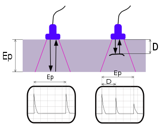
Ultrasonic testing (UT) is a family of non-destructive testing techniques based on the propagation of ultrasonic waves in the object or material tested. In most common UT applications, very short ultrasonic pulse-waves with center frequencies ranging from 0.1-15 MHz, and occasionally up to 50 MHz, are transmitted into materials to detect internal flaws or to characterize materials. A common example is ultrasonic thickness measurement, which tests the thickness of the test object, for example, to monitor pipework corrosion.

Near-field scanning optical microscopy (NSOM) or scanning near-field optical microscopy (SNOM) is a microscopy technique for nanostructure investigation that breaks the far field resolution limit by exploiting the properties of evanescent waves. In SNOM, the excitation laser light is focused through an aperture with a diameter smaller than the excitation wavelength, resulting in an evanescent field on the far side of the aperture. When the sample is scanned at a small distance below the aperture, the optical resolution of transmitted or reflected light is limited only by the diameter of the aperture. In particular, lateral resolution of 6 nm and vertical resolution of 2–5 nm have been demonstrated.
Nanophotonics or nano-optics is the study of the behavior of light on the nanometer scale, and of the interaction of nanometer-scale objects with light. It is a branch of optics, optical engineering, electrical engineering, and nanotechnology. It often involves dielectric structures such as nanoantennas, or metallic components, which can transport and focus light via surface plasmon polaritons.

A scanning acoustic microscope (SAM) is a device which uses focused sound to investigate, measure, or image an object. It is commonly used in failure analysis and non-destructive evaluation. It also has applications in biological and medical research. The semiconductor industry has found the SAM useful in detecting voids, cracks, and delaminations within microelectronic packages.
Acoustic microscopy is microscopy that employs very high or ultra high frequency ultrasound. Acoustic microscopes operate non-destructively and penetrate most solid materials to make visible images of internal features, including defects such as cracks, delaminations and voids.

Piezoresponse force microscopy (PFM) is a variant of atomic force microscopy (AFM) that allows imaging and manipulation of piezoelectric/ferroelectric materials domains. This is achieved by bringing a sharp conductive probe into contact with a ferroelectric surface and applying an alternating current (AC) bias to the probe tip in order to excite deformation of the sample through the converse piezoelectric effect (CPE). The resulting deflection of the probe cantilever is detected through standard split photodiode detector methods and then demodulated by use of a lock-in amplifier (LiA). In this way topography and ferroelectric domains can be imaged simultaneously with high resolution.
In microscopy, scanning joule expansion microscopy (SJEM) is a form of scanning probe microscopy heavily based on atomic force microscopy (AFM) that maps the temperature distribution along a surface. Resolutions down to 10 nm have been achieved and 1 nm resolution is theoretically possible. Thermal measurements at the nanometer scale are of both academic and industrial interest, particularly in regards to nanomaterials and modern integrated circuits.

Photoconductive atomic force microscopy (PC-AFM) is a variant of atomic force microscopy that measures photoconductivity in addition to surface forces.
The technique of vibrational analysis with scanning probe microscopy allows probing vibrational properties of materials at the submicrometer scale, and even of individual molecules. This is accomplished by integrating scanning probe microscopy (SPM) and vibrational spectroscopy. This combination allows for much higher spatial resolution than can be achieved with conventional Raman/FTIR instrumentation. The technique is also nondestructive, requires non-extensive sample preparation, and provides more contrast such as intensity contrast, polarization contrast and wavelength contrast, as well as providing specific chemical information and topography images simultaneously.

Atomic force acoustic microscopy (AFAM) is a type of scanning probe microscopy (SPM). It is a combination of acoustics and atomic force microscopy. The principal difference between AFAM and other forms of SPM is the addition of a transducer at the bottom of the sample which induces longitudinal out-of-plane vibrations in the specimen. These vibrations are sensed by a cantilever and tip called a probe. The figure shown here is the clear schematic of AFAM principle here B is the magnified version of the tip and sample placed on the transducer and tip having some optical coating generally gold coating to reflect the laser light on to the photodiode.
AFM-IR or infrared nanospectroscopy is one of a family of techniques that are derived from a combination of two parent instrumental techniques. AFM-IR combines the chemical analysis power of infrared spectroscopy and the high-spatial resolution of scanning probe microscopy (SPM). The term was first used to denote a method that combined a tuneable free electron laser with an atomic force microscope equipped with a sharp probe that measured the local absorption of infrared light by a sample with nanoscale spatial resolution.

Nano-FTIR is a scanning probe technique that utilizes as a combination of two techniques: Fourier transform infrared spectroscopy (FTIR) and scattering-type scanning near-field optical microscopy (s-SNOM). As s-SNOM, nano-FTIR is based on atomic-force microscopy (AFM), where a sharp tip is illuminated by an external light source and the tip-scattered light is detected as a function of tip position. A typical nano-FTIR setup thus consists of an atomic force microscope, a broadband infrared light source used for tip illumination, and a Michelson interferometer acting as Fourier-transform spectrometer. In nano-FTIR, the sample stage is placed in one of the interferometer arms, which allows for recording both amplitude and phase of the detected light. Scanning the tip allows for performing hyperspectral imaging with nanoscale spatial resolution determined by the tip apex size. The use of broadband infrared sources enables the acquisition of continuous spectra, which is a distinctive feature of nano-FTIR compared to s-SNOM. Nano-FTIR is capable of performing infrared (IR) spectroscopy of materials in ultrasmall quantities and with nanoscale spatial resolution. The detection of a single molecular complex and the sensitivity to a single monolayer has been shown. Recording infrared spectra as a function of position can be used for nanoscale mapping of the sample chemical composition, performing a local ultrafast IR spectroscopy and analyzing the nanoscale intermolecular coupling, among others. A spatial resolution of 10 nm to 20 nm is routinely achieved.
Super-resolution photoacoustic imaging is a set of techniques used to enhance spatial resolution in photoacoustic imaging. Specifically, these techniques primarily break the optical diffraction limit of the photoacoustic imaging system. It can be achieved in a variety of mechanisms, such as blind structured illumination, multi-speckle illumination, or photo-imprint photoacoustic microscopy in Figure 1.

Photoacoustic microscopy is an imaging method based on the photoacoustic effect and is a subset of photoacoustic tomography. Photoacoustic microscopy takes advantage of the local temperature rise that occurs as a result of light absorption in tissue. Using a nanosecond pulsed laser beam, tissues undergo thermoelastic expansion, resulting in the release of a wide-band acoustic wave that can be detected using a high-frequency ultrasound transducer. Since ultrasonic scattering in tissue is weaker than optical scattering, photoacoustic microscopy is capable of achieving high-resolution images at greater depths than conventional microscopy methods. Furthermore, photoacoustic microscopy is especially useful in the field of biomedical imaging due to its scalability. By adjusting the optical and acoustic foci, lateral resolution may be optimized for the desired imaging depth.
A probe tip is an instrument used in scanning probe microscopes (SPMs) to scan the surface of a sample and make nano-scale images of surfaces and structures. The probe tip is mounted on the end of a cantilever and can be as sharp as a single atom. In microscopy, probe tip geometry and the composition of both the tip and the surface being probed directly affect resolution and imaging quality. Tip size and shape are extremely important in monitoring and detecting interactions between surfaces. SPMs can precisely measure electrostatic forces, magnetic forces, chemical bonding, Van der Waals forces, and capillary forces. SPMs can also reveal the morphology and topography of a surface.
