MEMS is the technology of microscopic devices incorporating both electronic and moving parts. MEMS are made up of components between 1 and 100 micrometres in size, and MEMS devices generally range in size from 20 micrometres to a millimetre, although components arranged in arrays can be more than 1000 mm2. They usually consist of a central unit that processes data and several components that interact with the surroundings.

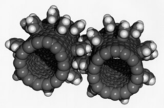
Nanotechnology is the manipulation of matter with at least one dimension sized from 1 to 100 nanometers (nm). At this scale, commonly known as the nanoscale, surface area and quantum mechanical effects become important in describing properties of matter. This definition of nanotechnology includes all types of research and technologies that deal with these special properties. It is common to see the plural form "nanotechnologies" as well as "nanoscale technologies" to refer to research and applications whose common trait is scale. An earlier understanding of nanotechnology referred to the particular technological goal of precisely manipulating atoms and molecules for fabricating macroscale products, now referred to as molecular nanotechnology.

Semiconductor device fabrication is the process used to manufacture semiconductor devices, typically integrated circuits (ICs) such as microprocessors, microcontrollers, and memories. It is a multiple-step photolithographic and physico-chemical process during which electronic circuits are gradually created on a wafer, typically made of pure single-crystal semiconducting material. Silicon is almost always used, but various compound semiconductors are used for specialized applications.
A nanowire is a nanostructure in the form of a wire with the diameter of the order of a nanometre (10−9 m). More generally, nanowires can be defined as structures that have a thickness or diameter constrained to tens of nanometers or less and an unconstrained length. At these scales, quantum mechanical effects are important—which coined the term "quantum wires".

A molecular assembler, as defined by K. Eric Drexler, is a "proposed device able to guide chemical reactions by positioning reactive molecules with atomic precision". A molecular assembler is a kind of molecular machine. Some biological molecules such as ribosomes fit this definition. This is because they receive instructions from messenger RNA and then assemble specific sequences of amino acids to construct protein molecules. However, the term "molecular assembler" usually refers to theoretical human-made devices.
Nanosensors are nanoscale devices that measure physical quantities and convert these to signals that can be detected and analyzed. There are several ways proposed today to make nanosensors; these include top-down lithography, bottom-up assembly, and molecular self-assembly. There are different types of nanosensors in the market and in development for various applications, most notably in defense, environmental, and healthcare industries. These sensors share the same basic workflow: a selective binding of an analyte, signal generation from the interaction of the nanosensor with the bio-element, and processing of the signal into useful metrics.
A lab-on-a-chip (LOC) is a device that integrates one or several laboratory functions on a single integrated circuit of only millimeters to a few square centimeters to achieve automation and high-throughput screening. LOCs can handle extremely small fluid volumes down to less than pico-liters. Lab-on-a-chip devices are a subset of microelectromechanical systems (MEMS) devices and sometimes called "micro total analysis systems" (μTAS). LOCs may use microfluidics, the physics, manipulation and study of minute amounts of fluids. However, strictly regarded "lab-on-a-chip" indicates generally the scaling of single or multiple lab processes down to chip-format, whereas "μTAS" is dedicated to the integration of the total sequence of lab processes to perform chemical analysis.

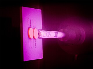
Physical vapor deposition (PVD), sometimes called physical vapor transport (PVT), describes a variety of vacuum deposition methods which can be used to produce thin films and coatings on substrates including metals, ceramics, glass, and polymers. PVD is characterized by a process in which the material transitions from a condensed phase to a vapor phase and then back to a thin film condensed phase. The most common PVD processes are sputtering and evaporation. PVD is used in the manufacturing of items which require thin films for optical, mechanical, electrical, acoustic or chemical functions. Examples include semiconductor devices such as thin-film solar cells, microelectromechanical devices such as thin film bulk acoustic resonator, aluminized PET film for food packaging and balloons, and titanium nitride coated cutting tools for metalworking. Besides PVD tools for fabrication, special smaller tools used mainly for scientific purposes have been developed.
Nanomanufacturing is both the production of nanoscaled materials, which can be powders or fluids, and the manufacturing of parts "bottom up" from nanoscaled materials or "top down" in smallest steps for high precision, used in several technologies such as laser ablation, etching and others. Nanomanufacturing differs from molecular manufacturing, which is the manufacture of complex, nanoscale structures by means of nonbiological mechanosynthesis.

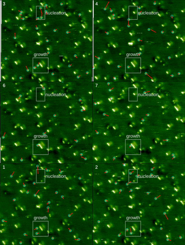
In chemistry and materials science, molecular self-assembly is the process by which molecules adopt a defined arrangement without guidance or management from an outside source. There are two types of self-assembly: intermolecular and intramolecular. Commonly, the term molecular self-assembly refers to the former, while the latter is more commonly called folding.
Molecular wires are molecular chains that conduct electric current. They are the proposed building blocks for molecular electronic devices. Their typical diameters are less than three nanometers, while their lengths may be macroscopic, extending to centimeters or more.

A biointerface is the region of contact between a biomolecule, cell, biological tissue or living organism or organic material considered living with another biomaterial or inorganic/organic material. The motivation for biointerface science stems from the urgent need to increase the understanding of interactions between biomolecules and surfaces. The behavior of complex macromolecular systems at materials interfaces are important in the fields of biology, biotechnology, diagnostics, and medicine. Biointerface science is a multidisciplinary field in which biochemists who synthesize novel classes of biomolecules cooperate with scientists who have developed the tools to position biomolecules with molecular precision, scientists who have developed new spectroscopic techniques to interrogate these molecules at the solid-liquid interface, and people who integrate these into functional devices. Well-designed biointerfaces would facilitate desirable interactions by providing optimized surfaces where biological matter can interact with other inorganic or organic materials, such as by promoting cell and tissue adhesion onto a surface.

Local oxidation nanolithography (LON) is a tip-based nanofabrication method. It is based on the spatial confinement on an oxidation reaction under the sharp tip of an atomic force microscope.
Self-assembling peptides are a category of peptides which undergo spontaneous assembling into ordered nanostructures. Originally described in 1993, these designer peptides have attracted interest in the field of nanotechnology for their potential for application in areas such as biomedical nanotechnology, tissue cell culturing, molecular electronics, and more.
Nanofluidic circuitry is a nanotechnology aiming for control of fluids in nanometer scale. Due to the effect of an electrical double layer within the fluid channel, the behavior of nanofluid is observed to be significantly different compared with its microfluidic counterparts. Its typical characteristic dimensions fall within the range of 1–100 nm. At least one dimension of the structure is in nanoscopic scale. Phenomena of fluids in nano-scale structure are discovered to be of different properties in electrochemistry and fluid dynamics.
Ultra-high-purity steam, also called the clean steam, UHP steam or high purity water vapor, is used in a variety of industrial manufacturing processes that require oxidation or annealing. These processes include the growth of oxide layers on silicon wafers for the semiconductor industry, originally described by the Deal-Grove model, and for the formation of passivation layers used to improve the light capture ability of crystalline photovoltaic cells. Several methods and technologies can be employed to generate ultra high purity steam, including pyrolysis, bubbling, direct liquid injection, and purified steam generation. The level of purity, or the relative lack of contamination, affects the quality of the oxide layer or annealed surface. The method of delivery affects growth rate, uniformity, and electrical performance. Oxidation and annealing are common steps in the manufacture of such devices as microelectronics and solar cells.
Membrane technology encompasses the scientific processes used in the construction and application of membranes. Membranes are used to facilitate the transport or rejection of substances between mediums, and the mechanical separation of gas and liquid streams. In the simplest case, filtration is achieved when the pores of the membrane are smaller than the diameter of the undesired substance, such as a harmful microorganism. Membrane technology is commonly used in industries such as water treatment, chemical and metal processing, pharmaceuticals, biotechnology, the food industry, as well as the removal of environmental pollutants.
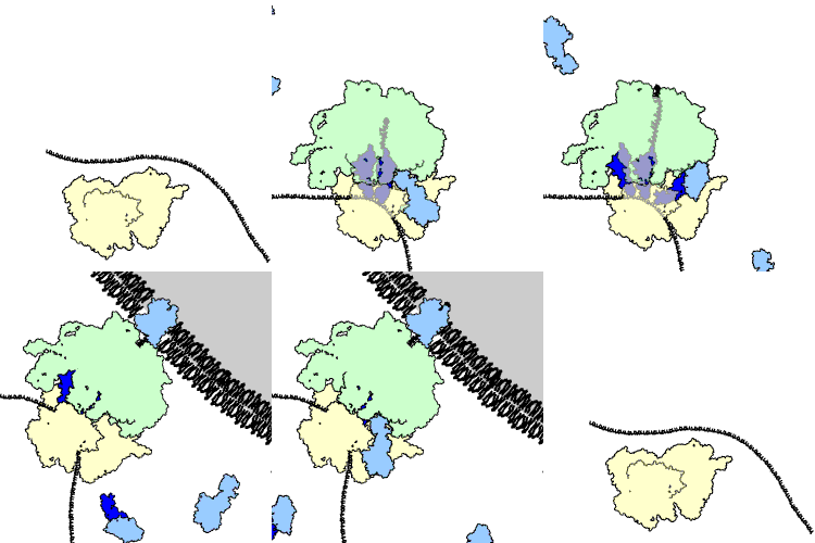
Atomic Terrace Low Angle Shadowing (ATLAS) is a surface science technique which enables the growth of planar nanowire or nanodot arrays using molecular beam epitaxy on a vicinal surface. ATLAS utilises the inherent step-and-terrace structure of the surface as a template for such nanostructures. The technique involves the low angle incidence of flux material on vicinal substrates. Vicinal substrates are composed of atomic terraces separated by atomic steps. The ATLAS technique allows for the fabrication of well defined planar arrays of plasmonic nanostructures, of dimensions unachievable by lithography.

Silicon nanowires, also referred to as SiNWs, are a type of semiconductor nanowire most often formed from a silicon precursor by etching of a solid or through catalyzed growth from a vapor or liquid phase. Such nanowires have promising applications in lithium-ion batteries, thermoelectrics and sensors. Initial synthesis of SiNWs is often accompanied by thermal oxidation steps to yield structures of accurately tailored size and morphology.
This glossary of nanotechnology is a list of definitions of terms and concepts relevant to nanotechnology, its sub-disciplines, and related fields.


