
Electronics is a scientific and engineering discipline that studies and applies the principles of physics to design, create, and operate devices that manipulate electrons and other electrically charged particles. It is a subfield of physics and electrical engineering which uses active devices such as transistors, diodes, and integrated circuits to control and amplify the flow of electric current and to convert it from one form to another, such as from alternating current (AC) to direct current (DC) or from analog signals to digital signals.

An integrated circuit (IC), also known as a microchip, computer chip, or simply chip, is a small electronic device made up of multiple interconnected electronic components such as transistors, resistors, and capacitors. These components are etched onto a small piece of semiconductor material, usually silicon. Integrated circuits are used in a wide range of electronic devices, including computers, smartphones, and televisions, to perform various functions such as processing and storing information. They have greatly impacted the field of electronics by enabling device miniaturization and enhanced functionality.

Semiconductor device fabrication is the process used to manufacture semiconductor devices, typically integrated circuits (ICs) such as computer processors, microcontrollers, and memory chips. It is a multiple-step photolithographic and physico-chemical process during which electronic circuits are gradually created on a wafer, typically made of pure single-crystal semiconducting material. Silicon is almost always used, but various compound semiconductors are used for specialized applications.

A transistor is a semiconductor device used to amplify or switch electrical signals and power. It is one of the basic building blocks of modern electronics. It is composed of semiconductor material, usually with at least three terminals for connection to an electronic circuit. A voltage or current applied to one pair of the transistor's terminals controls the current through another pair of terminals. Because the controlled (output) power can be higher than the controlling (input) power, a transistor can amplify a signal. Some transistors are packaged individually, but many more in miniature form are found embedded in integrated circuits. Because transistors are the key active components in practically all modern electronics, many people consider them one of the 20th century's greatest inventions.

A semiconductor device is an electronic component that relies on the electronic properties of a semiconductor material for its function. Its conductivity lies between conductors and insulators. Semiconductor devices have replaced vacuum tubes in most applications. They conduct electric current in the solid state, rather than as free electrons across a vacuum or as free electrons and ions through an ionized gas.

Complementary metal–oxide–semiconductor is a type of metal–oxide–semiconductor field-effect transistor (MOSFET) fabrication process that uses complementary and symmetrical pairs of p-type and n-type MOSFETs for logic functions. CMOS technology is used for constructing integrated circuit (IC) chips, including microprocessors, microcontrollers, memory chips, and other digital logic circuits. CMOS technology is also used for analog circuits such as image sensors, data converters, RF circuits, and highly integrated transceivers for many types of communication.

Gallium arsenide (GaAs) is a III-V direct band gap semiconductor with a zinc blende crystal structure.
A thin-film transistor (TFT) is a special type of field-effect transistor (FET) where the transistor is made by thin film deposition. TFTs are grown on a supporting substrate, such as glass. This differs from the conventional bulk metal oxide field effect transistor (MOSFET), where the semiconductor material typically is the substrate, such as a silicon wafer. The traditional application of TFTs is in TFT liquid-crystal displays.
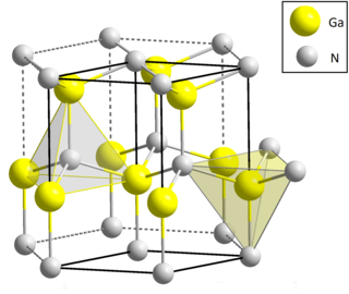
Gallium nitride is a binary III/V direct bandgap semiconductor commonly used in blue light-emitting diodes since the 1990s. The compound is a very hard material that has a Wurtzite crystal structure. Its wide band gap of 3.4 eV affords it special properties for applications in optoelectronic, high-power and high-frequency devices. For example, GaN is the substrate that makes violet (405 nm) laser diodes possible, without requiring nonlinear optical frequency doubling.
In computer engineering, a logic family is one of two related concepts:
Indium gallium arsenide (InGaAs) is a ternary alloy of indium arsenide (InAs) and gallium arsenide (GaAs). Indium and gallium are group III elements of the periodic table while arsenic is a group V element. Alloys made of these chemical groups are referred to as "III-V" compounds. InGaAs has properties intermediate between those of GaAs and InAs. InGaAs is a room-temperature semiconductor with applications in electronics and photonics.
Stanley Shanfield serves as a Distinguished Member of the Technical Staff and Technical Director of Advanced Hardware Development at the Charles Stark Draper Laboratory in Cambridge, Massachusetts, a post he has held since 2003. He is the holder of seven patents and has led teams responsible for inventing and manufacturing new technologies in the fields of semiconductor device fabrication and optical electronics.

In field-effect transistors (FETs), depletion mode and enhancement mode are two major transistor types, corresponding to whether the transistor is in an on state or an off state at zero gate–source voltage.

Jerry M. Woodall is a professor of electrical and computer engineering at the University of California, Davis who is widely known for his revolutionary work on LEDs and semiconductors. Over the course of his career, he has published close to 400 scientific articles and his work has directly contributed to the development of major technologies that are used around the world, such as TVs, optical fibers, and mobile phones. Woodall currently holds over 80 U.S. patents for a variety of inventions and has received prestigious awards from IBM, NASA, and the U.S. President for his contributions to science, technology, and humanity.
The first planar monolithic integrated circuit (IC) chip was demonstrated in 1960. The idea of integrating electronic circuits into a single device was born when the German physicist and engineer Werner Jacobi developed and patented the first known integrated transistor amplifier in 1949 and the British radio engineer Geoffrey Dummer proposed to integrate a variety of standard electronic components in a monolithic semiconductor crystal in 1952. A year later, Harwick Johnson filed a patent for a prototype IC. Between 1953 and 1957, Sidney Darlington and Yasuo Tarui proposed similar chip designs where several transistors could share a common active area, but there was no electrical isolation to separate them from each other.
Surface activated bonding (SAB) is a non-high-temperature wafer bonding technology with atomically clean and activated surfaces. Surface activation prior to bonding by using fast atom bombardment is typically employed to clean the surfaces. High-strength bonding of semiconductor, metal, and dielectric can be obtained even at room temperature.
Indium aluminium nitride (InAlN) is a direct bandgap semiconductor material used in the manufacture of electronic and photonic devices. It is part of the III-V group of semiconductors, being an alloy of indium nitride and aluminium nitride, and is closely related to the more widely used gallium nitride. It is of special interest in applications requiring good stability and reliability, owing to its large direct bandgap and ability to maintain operation at temperatures of up to 1000 °C., making it of particular interest to areas such as the space industry. InAlN high-electron-mobility transistors (HEMTs) are attractive candidates for such applications owing to the ability of InAlN to lattice-match to gallium nitride, eliminating a reported failure route in the closely related aluminium gallium nitride HEMTs.
Germanium-tin is an alloy of the elements germanium and tin, both located in group 14 of the periodic table. It is only thermodynamically stable under a small composition range. Despite this limitation, it has useful properties for band gap and strain engineering of silicon-integrated optoelectronic and microelectronic semiconductor devices.

Sanjay Banerjee is an American engineer at the University of Texas at Austin, director of Microelectronics Research Center, and director of the Southwest Academy of Nanoelectronics (SWAN) — one of three such centers in the United States funded by the Semiconductor Research Corporation to develop a replacement for MOSFETs as part of their Nanoelectronics Research Initiative (NRI).

Aristos Christou is an American engineer and scientist, academic professor and researcher. He is a Professor of Materials Science, Professor of Mechanical Engineering and Professor of Reliability Engineering at the University of Maryland.
