Stencil lithography

Last updated

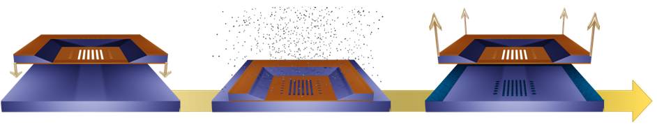
Stencil lithography is a novel method of fabricating nanometer scale patterns using nanostencils, stencils (shadow mask) with nanometer size apertures. It is a resist-less, simple, parallel nanolithography process, and it does not involve any heat or chemical treatment of the substrates (unlike resist-based techniques). StencilLithography.jpg

Contents

History

Stencil lithography was first reported in a scientific journal as a micro-structuring technique by S. Gray and P. K. Weimer in 1959. [1] They used long stretched metallic wires as shadow masks during metal deposition. Various materials can be used as membranes, such as metals, Si, SixNy, and polymers. Today the stencil apertures can be scaled down to sub-micrometer size at full 4" wafer scale. This is called a nanostencil. Nano-scale stencil apertures have been fabricated using laser interference lithography (LIL), electron beam lithography, and focused ion beam lithography.

Processes

Several process are available using stencil lithography: material deposition and etching, as well as implantation of ions. Different stencil requirements are necessary for the various processes, e. g. an extra etch-resistant layer on the backside of the stencil for etching (if the membrane material is sensitive to the etching process) or a conductive layer on the backside of the stencil for ion implantation.

Deposition

The main deposition method used with stencil lithography is physical vapor deposition. This includes thermal and electron beam physical vapor deposition, molecular beam epitaxy, sputtering, and pulsed laser deposition. The more directional the material flux is, the more accurate the pattern is transferred from the stencil to the substrate.

Etching

Reactive ion etching is based on ionized, accelerated particles that etch both chemically and physically the substrate. The stencil in this case is used as a hard mask, protecting the covered regions of the substrate, while allowing the substrate under the stencil apertures to be etched.

Ion implantation

Here the thickness of the membrane has to be greater than the penetration length of the ions in the membrane material. The ions will then implant only under the stencil apertures, into the substrate.

Modes

There are three main modes of operation of stencil lithography: static, quasi-dynamic and dynamic. While all the above described processes have been proven using the static mode (stencil doesn't move relative to substate during material or ion processing), only ion implantation has been shown for the non-static modes (quasi-dynamic).

Static stencil

In the static mode, the stencil is aligned (if necessary) and fixed to a substrate. The stencil-substrate pair is placed in the evaporation/etching/ion implantation machine, and after the processing is done, the stencil is simply removed from the now patterned substrate.

Quasi-dynamic stencil

In the quasi-dynamic mode (or step-and-repeat), the stencil moves relative to the substrate in between depositions, without breaking the vacuum.

Dynamic stencil

In the dynamic mode, the stencil moves relative to the substrate during deposition, allowing the fabrication of patterns with variable height profiles by changing the stencil speed during a constant material deposition rate. For motion in one-dimension, the deposited material has a height profile given by the convolution

where is the time the mask resides at longitudinal position , and is the constant deposition rate. represents the height profile that would be produced by a static immobile mask (inclusive of any blurring). Programmable-height nanostructures as small as 10nm can be produced. [2]

Challenges

Despite it being a versatile technique, there are still several challenges to be addressed by stencil lithography. During deposition through the stencil, material is deposited not only on the substrate through the apertures but also on the stencil backside, including around and inside the apertures. This reduces the effective aperture size by an amount proportional to the deposited material, leading ultimately to aperture clogging.

The accuracy of the pattern transfer from the stencil to the substrate depends on many parameters. The material diffusion on the substrate (as a function of temperature, material type, evaporation angle) and the geometrical setup of the evaporation are the main factors. Both lead to an enlargement of the initial pattern, called blurring.

See also

Related Research Articles

<span class="mw-page-title-main">Microelectromechanical systems</span> Very small devices that incorporate moving components

Microelectromechanical systems (MEMS), also written as micro-electro-mechanical systems and the related micromechatronics and microsystems constitute the technology of microscopic devices, particularly those with moving parts. They merge at the nanoscale into nanoelectromechanical systems (NEMS) and nanotechnology. MEMS are also referred to as micromachines in Japan and microsystem technology (MST) in Europe.

In integrated circuit manufacturing, photolithography or optical lithography is a general term used for techniques that use light to produce minutely patterned thin films of suitable materials over a substrate, such as a silicon wafer, to protect selected areas of it during subsequent etching, deposition, or implantation operations. Typically, ultraviolet light is used to transfer a geometric design from an optical mask to a light-sensitive chemical (photoresist) coated on the substrate. The photoresist either breaks down or hardens where it is exposed to light. The patterned film is then created by removing the softer parts of the coating with appropriate solvents.

<span class="mw-page-title-main">Photomask</span>

A photomask is an opaque plate with holes or transparencies that allow light to shine through in a defined pattern. They are commonly used in photolithography and the production of integrated circuits in particular. Masks are used to produce a pattern on a substrate, normally a thin slice of silicon known as a wafer in the case of chip manufacturing. Several masks are used in turn, each one reproducing a layer of the completed design, and together they are known as a mask set.

Surface micromachining builds microstructures by deposition and etching structural layers over a substrate. This is different from Bulk micromachining, in which a silicon substrate wafer is selectively etched to produce structures.

<span class="mw-page-title-main">Ion beam</span> Beam of charged atoms (ions)

An ion beam is a type of charged particle beam consisting of ions. Ion beams have many uses in electronics manufacturing and other industries. A variety of ion beam sources exists, some derived from the mercury vapor thrusters developed by NASA in the 1960s. The most common ion beams are of singly-charged ions.

Nanolithography (NL) is a growing field of techniques within nanotechnology dealing with the engineering of nanometer-scale structures on various materials.

<span class="mw-page-title-main">Dip-pen nanolithography</span> Scanning probe lithographic technique

Dip pen nanolithography (DPN) is a scanning probe lithography technique where an atomic force microscope (AFM) tip is used to create patterns directly on a range of substances with a variety of inks. A common example of this technique is exemplified by the use of alkane thiolates to imprint onto a gold surface. This technique allows surface patterning on scales of under 100 nanometers. DPN is the nanotechnology analog of the dip pen, where the tip of an atomic force microscope cantilever acts as a "pen," which is coated with a chemical compound or mixture acting as an "ink," and put in contact with a substrate, the "paper."

In semiconductor fabrication, a resist is a thin layer used to transfer a circuit pattern to the semiconductor substrate which it is deposited upon. A resist can be patterned via lithography to form a (sub)micrometer-scale, temporary mask that protects selected areas of the underlying substrate during subsequent processing steps. The material used to prepare said thin layer is typically a viscous solution. Resists are generally proprietary mixtures of a polymer or its precursor and other small molecules that have been specially formulated for a given lithography technology. Resists used during photolithography are called photoresists.

Deep reactive-ion etching (DRIE) is a highly anisotropic etch process used to create deep penetration, steep-sided holes and trenches in wafers/substrates, typically with high aspect ratios. It was developed for microelectromechanical systems (MEMS), which require these features, but is also used to excavate trenches for high-density capacitors for DRAM and more recently for creating through silicon vias (TSVs) in advanced 3D wafer level packaging technology. In DRIE, the substrate is placed inside a reactor, and several gases are introduced. A plasma is struck in the gas mixture which breaks the gas molecules into ions. The ions accelerated towards, and react with the surface of the material being etched, forming another gaseous element. This is known as the chemical part of the reactive ion etching. There is also a physical part, if ions have enough energy, they can knock atoms out of the material to be etched without chemical reaction.

<span class="mw-page-title-main">Microfabrication</span>

Microfabrication is the process of fabricating miniature structures of micrometre scales and smaller. Historically, the earliest microfabrication processes were used for integrated circuit fabrication, also known as "semiconductor manufacturing" or "semiconductor device fabrication". In the last two decades microelectromechanical systems (MEMS), microsystems, micromachines and their subfields, microfluidics/lab-on-a-chip, optical MEMS, RF MEMS, PowerMEMS, BioMEMS and their extension into nanoscale have re-used, adapted or extended microfabrication methods. Flat-panel displays and solar cells are also using similar techniques.

<span class="mw-page-title-main">Optical proximity correction</span> Photolithography enhancement technique

Optical proximity correction (OPC) is a photolithography enhancement technique commonly used to compensate for image errors due to diffraction or process effects. The need for OPC is seen mainly in the making of semiconductor devices and is due to the limitations of light to maintain the edge placement integrity of the original design, after processing, into the etched image on the silicon wafer. These projected images appear with irregularities such as line widths that are narrower or wider than designed, these are amenable to compensation by changing the pattern on the photomask used for imaging. Other distortions such as rounded corners are driven by the resolution of the optical imaging tool and are harder to compensate for. Such distortions, if not corrected for, may significantly alter the electrical properties of what was being fabricated. Optical proximity correction corrects these errors by moving edges or adding extra polygons to the pattern written on the photomask. This may be driven by pre-computed look-up tables based on width and spacing between features or by using compact models to dynamically simulate the final pattern and thereby drive the movement of edges, typically broken into sections, to find the best solution,. The objective is to reproduce on the semiconductor wafer, as well as possible, the original layout drawn by the designer.

Chemical beam epitaxy (CBE) forms an important class of deposition techniques for semiconductor layer systems, especially III-V semiconductor systems. This form of epitaxial growth is performed in an ultrahigh vacuum system. The reactants are in the form of molecular beams of reactive gases, typically as the hydride or a metalorganic. The term CBE is often used interchangeably with metal-organic molecular beam epitaxy (MOMBE). The nomenclature does differentiate between the two processes, however. When used in the strictest sense, CBE refers to the technique in which both components are obtained from gaseous sources, while MOMBE refers to the technique in which the group III component is obtained from a gaseous source and the group V component from a solid source.

<span class="mw-page-title-main">LIGA</span> Fabrication technology used to create high-aspect-ratio microstructures

LIGA is a fabrication technology used to create high-aspect-ratio microstructures. The term is a German acronym for Lithographie, Galvanoformung, Abformung – lithography, electroplating, and molding.

Electron-beam physical vapor deposition, or EBPVD, is a form of physical vapor deposition in which a target anode is bombarded with an electron beam given off by a charged tungsten filament under high vacuum. The electron beam causes atoms from the target to transform into the gaseous phase. These atoms then precipitate into solid form, coating everything in the vacuum chamber with a thin layer of the anode material.

<span class="mw-page-title-main">Multiple patterning</span> Technique used to increase the number of structures a microchip may contain

Multiple patterning is a class of technologies for manufacturing integrated circuits (ICs), developed for photolithography to enhance the feature density. It is expected to be necessary for the 10 nm and 7 nm node semiconductor processes and beyond. The premise is that a single lithographic exposure may not be enough to provide sufficient resolution. Hence additional exposures would be needed, or else positioning patterns using etched feature sidewalls would be necessary.

<span class="mw-page-title-main">Etching (microfabrication)</span> Technique in microfabrication used to remove material and create structures

Etching is used in microfabrication to chemically remove layers from the surface of a wafer during manufacturing. Etching is a critically important process module, and every wafer undergoes many etching steps before it is complete.

Patterned media is a potential future hard disk drive technology to record data in magnetic islands, as opposed to current hard disk drive technology where each bit is stored in 20–30 magnetic grains within a continuous magnetic film. The islands would be patterned from a precursor magnetic film using nanolithography. It is one of the proposed technologies to succeed perpendicular recording due to the greater storage densities it would enable. BPM was introduced by Toshiba in 2010.

The lift-off process in microstructuring technology is a method of creating structures (patterning) of a target material on the surface of a substrate using a sacrificial material . It is an additive technique as opposed to more traditional subtracting technique like etching. The scale of the structures can vary from the nanoscale up to the centimeter scale or further, but are typically of micrometric dimensions.

<span class="mw-page-title-main">Nanochannel glass materials</span> Novel mask technology

Nanochannel glass materials are an experimental mask technology that is an alternate method for fabricating nanostructures, although optical lithography is the predominant patterning technique.

Glossary of microelectronics manufacturing terms

References

  1. Gray, S; Weimer, PK (1959). "Production Of Fine Patterns By Evaporation". RCA Review. RCA Corporation. 20 (3): 413–425. ISSN   0033-6831.
  2. J. L. Wasserman; et al. (2008). "Fabrication of One-Dimensional Programmable-Height Nanostructures via Dynamic Stencil Deposition". Review of Scientific Instruments . 79: 073909. arXiv: 0802.1848 . Bibcode:2008RScI...79g3909W. doi:10.1063/1.2960573. PMID   18681718.

Series in MICROSYSTEMS Vol. 20: Marc Antonius Friedrich van den Boogaart, "Stencil lithography: An ancient technique for advanced micro- and nanopatterning", 2006, VIII, 182 p.; ISBN   3-86628-110-2