
Diffraction is the deviation of waves from straight-line propagation due to an obstacle or through an aperture. The diffracting object or aperture effectively becomes a secondary source of the propagating wave. Diffraction is the same physical effect as interference, but interference is typically applied to superposition of a few waves and the term diffraction is used when many waves are superposed.
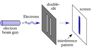
In modern physics, the double-slit experiment demonstrates that light and matter can exhibit behavior of both classical particles and classical waves. This type of experiment was first performed by Thomas Young in 1801, as a demonstration of the wave behavior of visible light. In 1927, Davisson and Germer and, independently, George Paget Thomson and his research student Alexander Reid demonstrated that electrons show the same behavior, which was later extended to atoms and molecules. Thomas Young's experiment with light was part of classical physics long before the development of quantum mechanics and the concept of wave–particle duality. He believed it demonstrated that the Christiaan Huygens' wave theory of light was correct, and his experiment is sometimes referred to as Young's experiment or Young's slits.

In physics, interference is a phenomenon in which two coherent waves are combined by adding their intensities or displacements with due consideration for their phase difference. The resultant wave may have greater intensity or lower amplitude if the two waves are in phase or out of phase, respectively. Interference effects can be observed with all types of waves, for example, light, radio, acoustic, surface water waves, gravity waves, or matter waves as well as in loudspeakers as electrical waves.
Photolithography is a process used in the manufacturing of integrated circuits. It involves using light to transfer a pattern onto a substrate, typically a silicon wafer.
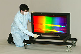
In optics, a diffraction grating is an optical grating with a periodic structure that diffracts light, or another type of electromagnetic radiation, into several beams traveling in different directions. The emerging coloration is a form of structural coloration. The directions or diffraction angles of these beams depend on the wave (light) incident angle to the diffraction grating, the spacing or periodic distance between adjacent diffracting elements on the grating, and the wavelength of the incident light. The grating acts as a dispersive element. Because of this, diffraction gratings are commonly used in monochromators and spectrometers, but other applications are also possible such as optical encoders for high-precision motion control and wavefront measurement.

Holography is a technique that enables a wavefront to be recorded and later reconstructed. It is best known as a method of generating three-dimensional images, and has a wide range of other uses, including data storage, microscopy, and interferometry. In principle, it is possible to make a hologram for any type of wave.
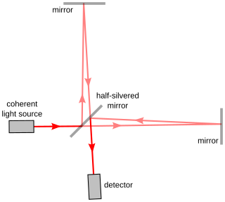
Interferometry is a technique which uses the interference of superimposed waves to extract information. Interferometry typically uses electromagnetic waves and is an important investigative technique in the fields of astronomy, fiber optics, engineering metrology, optical metrology, oceanography, seismology, spectroscopy, quantum mechanics, nuclear and particle physics, plasma physics, biomolecular interactions, surface profiling, microfluidics, mechanical stress/strain measurement, velocimetry, optometry, and making holograms.
The photorefractive effect is a nonlinear optical effect seen in certain crystals and other materials that respond to light by altering their refractive index. The effect can be used to store temporary, erasable holograms and is useful for holographic data storage. It can also be used to create a phase-conjugate mirror or an optical spatial soliton.
Masklesslithography (MPL) is a photomask-less photolithography-like technology used to project or focal-spot write the image pattern onto a chemical resist-coated substrate by means of UV radiation or electron beam.
Nanolithography (NL) is a growing field of techniques within nanotechnology dealing with the engineering of nanometer-scale structures on various materials.
Nanoimprint lithography (NIL) is a method of fabricating nanometer-scale patterns. It is a simple nanolithography process with low cost, high throughput and high resolution. It creates patterns by mechanical deformation of imprint resist and subsequent processes. The imprint resist is typically a monomer or polymer formulation that is cured by heat or UV light during the imprinting. Adhesion between the resist and the template is controlled to allow proper release.
Contact lithography, also known as contact printing, is a form of photolithography whereby the image to be printed is obtained by illumination of a photomask in direct contact with a substrate coated with an imaging photoresist layer.
Lloyd's mirror is an optics experiment that was first described in 1834 by Humphrey Lloyd in the Transactions of the Royal Irish Academy. Its original goal was to provide further evidence for the wave nature of light, beyond those provided by Thomas Young and Augustin-Jean Fresnel. In the experiment, light from a monochromatic slit source reflects from a glass surface at a small angle and appears to come from a virtual source as a result. The reflected light interferes with the direct light from the source, forming interference fringes. It is the optical wave analogue to a sea interferometer.
A distributed-feedback laser (DFB) is a type of laser diode, quantum-cascade laser or optical-fiber laser where the active region of the device contains a periodically structured element or diffraction grating. The structure builds a one-dimensional interference grating, and the grating provides optical feedback for the laser. This longitudinal diffraction grating has periodic changes in refractive index that cause reflection back into the cavity. The periodic change can be either in the real part of the refractive index or in the imaginary part. The strongest grating operates in the first order, where the periodicity is one-half wave, and the light is reflected backwards. DFB lasers tend to be much more stable than Fabry–Perot or DBR lasers and are used frequently when clean single-mode operation is needed, especially in high-speed fiber-optic telecommunications. Semiconductor DFB lasers in the lowest loss window of optical fibers at about 1.55 μm wavelength, amplified by erbium-doped fiber amplifiers (EDFAs), dominate the long-distance communication market, while DFB lasers in the lowest dispersion window at 1.3 μm are used at shorter distances.
Computer-generated holography (CGH) is a technique that uses computer algorithms to generate holograms. It involves generating holographic interference patterns. A computer-generated hologram can be displayed on a dynamic holographic display, or it can be printed onto a mask or film using lithography. When a hologram is printed onto a mask or film, it is then illuminated by a coherent light source to display the holographic images.
Microlithography is a general name for any manufacturing process that can create a minutely patterned thin film of protective materials over a substrate, such as a silicon wafer, in order to protect selected areas of it during subsequent etching, deposition, or implantation operations. The term is normally used for processes that can reliably produce features of microscopic size, such as 10 micrometres or less. The term nanolithography may be used to designate processes that can produce nanoscale features, such as less than 100 nanometres.
The Kapitza–Dirac effect is a quantum mechanical effect consisting of the diffraction of matter by a standing wave of light, in complete analogy to the diffraction of light by a periodic grating, but with the role of matter and light reversed. The effect was first predicted as the diffraction of electrons from a standing wave of light by Paul Dirac and Pyotr Kapitsa in 1933. The effect relies on the wave–particle duality of matter as stated by the de Broglie hypothesis in 1924. The matter-wave diffraction by a standing wave of light was first observed using a beam of neutral atoms. Later, the Kapitza-Dirac effect as originally proposed was observed in 2001.
Plasmonic nanolithography is a nanolithographic process that utilizes surface plasmon excitations such as surface plasmon polaritons (SPPs) to fabricate nanoscale structures. SPPs, which are surface waves that propagate in between planar dielectric-metal layers in the optical regime, can bypass the diffraction limit on the optical resolution that acts as a bottleneck for conventional photolithography.
Optical holography is a technique which enables an optical wavefront to be recorded and later re-constructed. Holography is best known as a method of generating three-dimensional images but it also has a wide range of other applications.
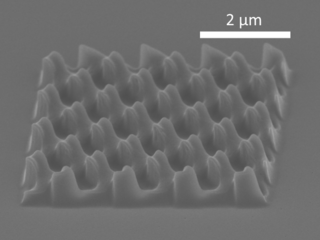
In materials science, Direct Laser Interference Patterning (DLIP) is a laser-based technology that uses the physical principle of interference of high-intensity, coherent laser pulses to produce functional periodic microstructures. To achieve interference, the beam is divided by a beam splitter, specialized prisms, or other elements. The beams are then overlapped on amaterial surface to form an interference pattern. If the power of the laser beam is sufficiently high, material removal can occur at the interference maxima through processes such as remelting, evaporation and ablation, while the material at the interference minima remains mostly intact. In this way, a large variety of periodic patterns can be created on the surface of the material. Depending on the lasers used, DLIP can be applied to almost any material and can change the properties of surfaces in many technological areas with regard to electrical and optical properties, tribology (friction and wear), light absorption and wettability.


