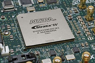
A field-programmable gate array (FPGA) is an integrated circuit designed to be configured by a customer or a designer after manufacturing – hence the term field-programmable. The FPGA configuration is generally specified using a hardware description language (HDL), similar to that used for an application-specific integrated circuit (ASIC). Circuit diagrams were previously used to specify the configuration, but this is increasingly rare due to the advent of electronic design automation tools.

A programmable logic device (PLD) is an electronic component used to build reconfigurable digital circuits. Unlike digital logic constructed using discrete logic gates with fixed functions, a PLD has an undefined function at the time of manufacture. Before the PLD can be used in a circuit it must be programmed to implement the desired function. Compared to fixed logic devices, programmable logic devices simplify the design of complex logic and may offer superior performance. Unlike for microprocessors, programming a PLD changes the connections made between the gates in the device.

A system on a chip, also written as system-on-a-chip and system-on-chip, is an integrated circuit that integrates all or most components of a computer or other electronic system. These components almost always include a central processing unit (CPU), memory interfaces, on-chip input/output devices and secondary storage interfaces, often alongside other components such as radio modems and a graphics processing unit (GPU) – all on a single substrate or microchip. It may contain digital, analog, mixed-signal, and often radio frequency signal processing functions.

An application-specific integrated circuit is an integrated circuit (IC) chip customized for a particular use, rather than intended for general-purpose use. For example, a chip designed to run in a digital voice recorder or a high-efficiency video codec is an ASIC. Application-specific standard product (ASSP) chips are intermediate between ASICs and industry standard integrated circuits like the 7400 series or the 4000 series. ASIC chips are typically fabricated using metal-oxide-semiconductor (MOS) technology, as MOS integrated circuit chips.
Reconfigurable computing is a computer architecture combining some of the flexibility of software with the high performance of hardware by processing with very flexible high speed computing fabrics like field-programmable gate arrays (FPGAs). The principal difference when compared to using ordinary microprocessors is the ability to make substantial changes to the datapath itself in addition to the control flow. On the other hand, the main difference from custom hardware, i.e. application-specific integrated circuits (ASICs) is the possibility to adapt the hardware during runtime by "loading" a new circuit on the reconfigurable fabric.

Altera Corporation was a manufacturer of programmable logic devices (PLDs) headquartered in San Jose, California. It was founded in 1983 and acquired by Intel in 2015.

A gate array is an approach to the design and manufacture of application-specific integrated circuits (ASICs) using a prefabricated chip with components that are later interconnected into logic devices according to a custom order by adding metal interconnect layers in the factory. It was popular during upheaval in semiconductor industry in 80s and its usage declined by end of 90s.
JTAG is an industry standard for verifying designs and testing printed circuit boards after manufacture.

A complex programmable logic device (CPLD) is a programmable logic device with complexity between that of PALs and FPGAs, and architectural features of both. The main building block of the CPLD is a macrocell, which contains logic implementing disjunctive normal form expressions and more specialized logic operations.
LEON is a radiation-tolerant 32-bit central processing unit (CPU) microprocessor core that implements the SPARC V8 instruction set architecture (ISA) developed by Sun Microsystems. It was originally designed by the European Space Research and Technology Centre (ESTEC), part of the European Space Agency (ESA), and after a short lifespan at Gaisler Research. It is described in synthesizable VHSIC Hardware Description Language (VHDL). LEON has a dual license model: An GNU Lesser General Public License (LGPL) and GNU General Public License (GPL) free and open-source software (FOSS) license that can be used without licensing fee, or a proprietary license that can be purchased for integration in a proprietary product. The core is configurable through VHDL generics, and is used in system on a chip (SOC) designs both in research and commercial settings.
Nios II is a 32-bit embedded processor architecture designed specifically for the Altera family of field-programmable gate array (FPGA) integrated circuits. Nios II incorporates many enhancements over the original Nios architecture, making it more suitable for a wider range of embedded computing applications, from digital signal processing (DSP) to system-control.

PSoC is a family of microcontroller integrated circuits by Cypress Semiconductor. These chips include a CPU core and mixed-signal arrays of configurable integrated analog and digital peripherals.
Actel Corporation was an American manufacturer of nonvolatile, low-power field-programmable gate arrays (FPGAs), mixed-signal FPGAs, and programmable logic solutions. It was headquartered in Mountain View, California, with offices worldwide. In November 2010, Actel was acquired by Microsemi for $430 million.
LatticeMico32 is a 32-bit microprocessor reduced instruction set computer (RISC) soft core from Lattice Semiconductor optimized for field-programmable gate arrays (FPGAs). It uses a Harvard architecture, which means the instruction and data buses are separate. Bus arbitration logic can be used to combine the two buses, if desired.
Aldec, Inc. is a privately owned electronic design automation company based in Henderson, Nevada that provides software and hardware used in creation and verification of digital designs targeting FPGA and ASIC technologies.
An application-specific instruction set processor (ASIP) is a component used in system-on-a-chip design. The instruction set of an ASIP is tailored to benefit a specific application. This specialization of the core provides a tradeoff between the flexibility of a general purpose CPU and the performance of an ASIC.
Field-programmable gate array prototyping, also referred to as FPGA-based prototyping, ASIC prototyping or system-on-chip (SoC) prototyping, is the method to prototype system-on-chip and application-specific integrated circuit designs on FPGAs for hardware verification and early software development.
eSi-RISC is a configurable CPU architecture. It is available in five implementations: the eSi-1600, eSi-1650, eSi-3200, eSi-3250 and eSi-3264. The eSi-1600 and eSi-1650 feature a 16-bit data-path, while the eSi-32x0s feature 32-bit data-paths, and the eSi-3264 features a mixed 32/64-bit datapath. Each of these processors is licensed as soft IP cores, suitable for integrating into both ASICs and FPGAs.
The Xputer is a design for a reconfigurable computer, proposed by computer scientist Reiner Hartenstein. Hartenstein uses various terms to describe the various innovations in the design, including config-ware, flow-ware, morph-ware, and "anti-machine".
In computing, a logic block or configurable logic block (CLB) is a fundamental building block of field-programmable gate array (FPGA) technology. Logic blocks can be configured by the engineer to provide reconfigurable logic gates.


