Surface reconstruction refers to the process by which atoms at the surface of a crystal assume a different structure than that of the bulk. Surface reconstructions are important in that they help in the understanding of surface chemistry for various materials, especially in the case where another material is adsorbed onto the surface.
In an ideal infinite crystal, the equilibrium position of each individual atom is determined by the forces exerted by all the other atoms in the crystal, resulting in a periodic structure. If a surface is introduced to the surroundings by terminating the crystal along a given plane, then these forces are altered, changing the equilibrium positions of the remaining atoms. This is most noticeable for the atoms at or near the surface plane, as they now only experience inter-atomic forces from one direction. This imbalance results in the atoms near the surface assuming positions with different spacing and/or symmetry from the bulk atoms, creating a different surface structure. This change in equilibrium positions near the surface can be categorized as either a relaxation or a reconstruction.
Surface relaxation
Relaxation refers to a change in the position of surface atoms relative to the bulk positions, while the bulk unit cell is preserved at the surface. Often this is a purely normal relaxation: that is, the surface atoms move in a direction normal to the surface plane, usually resulting in a smaller-than-usual inter-layer spacing. This makes intuitive sense, as a surface layer that experiences no forces from the open region can be expected to contract towards the bulk. Most metals experience this type of relaxation.[1] Some surfaces also experience relaxations in the lateral direction as well as the normal, so that the upper layers become shifted relative to layers further in, in order to minimize the positional energy.
A simple surface reconstruction
Reconstruction refers to a change in the two-dimensional structure of the surface layers, in addition to changes in the position of the entire layer. For example, in a cubic material the surface layer might re-structure itself to assume a smaller two-dimensional spacing between the atoms, as lateral forces from adjacent layers are reduced. The general symmetry of a layer might also change, as in the case of the Pt (100) surface, which reconstructs from a cubic to a hexagonal structure.[2] A reconstruction can affect one or more layers at the surface and can either conserve the total number of atoms in a layer (a conservative reconstruction) or have a greater or lesser number than in the bulk (a non-conservative reconstruction).
Reconstruction due to adsorption
The relaxations and reconstructions considered above would describe the ideal case of atomically clean surfaces in vacuum, in which the interaction with another medium is not considered. However, reconstructions can also be induced or affected by the adsorption of other atoms onto the surface, as the interatomic forces are changed. These reconstructions can assume a variety of forms when the detailed interactions between different types of atoms are taken into account, but some general principles can be identified.
The reconstruction of a surface with adsorption will depend on the following factors:
The composition of the substrate and of the adsorbate.
The coverage of the substrate surface layers and of the adsorbate, measured in monolayers.
The ambient conditions (i.e. temperature, gas pressure, etc.).
Composition plays an important role in that it determines the form that the adsorption process takes, whether by relatively weak physisorption through van der Waals interactions or stronger chemisorption through the formation of chemical bonds between the substrate and adsorbate atoms. Surfaces that undergo chemisorption generally result in more extensive reconstructions than those that undergo physisorption, as the breaking and formation of bonds between the surface atoms alter the interaction of the substrate atoms as well as the adsorbate.
Different reconstructions can also occur depending on the substrate and adsorbate coverages and the ambient conditions, as the equilibrium positions of the atoms are changed depending on the forces exerted. One example of this occurs in the case of In adsorbed on the Si(111) surface, in which the two differently reconstructed phases of Si(111)-In and Si(111)-In (in Wood's notation, see below) can actually coexist under certain conditions. These phases are distinguished by the In coverage in the different regions and occur for certain ranges of the average In coverage.[3]
Notation of reconstructions
In general, the change in a surface layer's structure due to a reconstruction can be completely specified by a matrix notation proposed by Park and Madden.[4] If and are the basic translation vectors of the two-dimensional structure in the bulk, and and are the basic translation vectors of the superstructure or reconstructed plane, then the relationship between the two sets of vectors can be described by the following equations:
so that the two-dimensional reconstruction can be described by the matrix[4]
Note that this system does not describe any relaxation of the surface layers relative to the bulk inter-layer spacing, but only describes the change in the individual layer's structure.
Surface reconstructions are more commonly given in Wood's notation, which reduces the matrix above into a more compact notation[5]
X(hkl) m × n - Rφ,
which describes the reconstruction of the (hkl) plane (given by its Miller indices). In this notation, the surface unit cell is given as multiples of the nonreconstructed surface unit cell with the unit cell vectors a and b. For example, a calcite(104) (2×1) reconstruction means that the unit cell is twice as long in direction a and has the same length in direction b. If the unit cell is rotated with respect to the unit cell of the nonreconstructed surface, the angle φ is given in addition (usually in degrees). This notation is often used to describe reconstructions concisely, but does not directly indicate changes in the layer symmetry (for example, square to hexagonal).
Measurement of reconstructions
Determination of a material's surface reconstruction requires a measurement of the positions of the surface atoms that can be compared to a measurement of the bulk structure. While the bulk structure of crystalline materials can usually be determined by using a diffraction experiment to determine the Bragg peaks, any signal from a reconstructed surface is obscured due to the relatively tiny number of atoms involved.
Special techniques are thus required to measure the positions of the surface atoms, and these generally fall into two categories: diffraction-based methods adapted for surface science, such as low-energy electron diffraction (LEED) or Rutherford backscattering spectroscopy, and atomic-scale probe techniques such as scanning tunneling microscopy (STM) or atomic force microscopy. Of these, STM has been most commonly used in recent history due to its very high resolution and ability to resolve aperiodic features.
Examples of reconstructions
To allow a better understanding of the variety of reconstructions in different systems, examine the following examples of reconstructions in metallic, semiconducting and insulating materials.
Silicon
A very well known example of surface reconstruction occurs in silicon, a semiconductor commonly used in a variety of computing and microelectronics applications. With a diamond-like face-centered cubic (fcc) lattice, it exhibits several different well-ordered reconstructions depending on temperature and on which crystal face is exposed.
When Si is cleaved along the (100) surface, the ideal diamond-like structure is interrupted and results in a 1×1 square array of surface Si atoms. Each of these has two dangling bonds remaining from the diamond structure, creating a surface that can obviously be reconstructed into a lower-energy structure. The observed reconstruction is a 2×1 periodicity, explained by the formation of dimers, which consist of paired surface atoms, decreasing the number of dangling bonds by a factor of two. These dimers reconstruct in rows with a high long-range order, resulting in a surface of filled and empty rows. LEED studies and calculations also indicate that relaxations as deep as five layers into the bulk are also likely to occur.[6]
The Si (111) structure, by comparison, exhibits a much more complex reconstruction. Cleavage along the (111) surface at low temperatures results in another 2×1 reconstruction, differing from the (100) surface by forming long π-bonded chains in the first and second surface layers. However, when heated above 400°C, this structure converts irreversibly to the more complicated 7×7 reconstruction. In addition, a disordered 1×1 structure is regained at temperatures above 850°C, which can be converted back to the 7×7 reconstruction by slow cooling.
The 7×7 reconstruction is modeled according to a dimer-adatom-stacking fault (DAS) model constructed by many research groups over a period of 25 years. Extending through the five top layers of the surface, the unit cell of the reconstruction contains 12 adatoms and 2 triangular subunits, 9 dimers, and a deep corner hole that extends to the fourth and fifth layers. This structure was gradually inferred from LEED and RHEED measurements and calculation, and was finally resolved in real space by Gerd Binnig, Heinrich Rohrer, Ch.Gerber and E.Weibel as a demonstration of the STM, which was developed by Binnig and Rohrer at IBM's Zurich Research Laboratory.[7] The full structure with positions of all reconstructed atoms has also been confirmed by massively parallel computation.[8]
A number of similar DAS reconstructions have also been observed on Si (111) in non-equilibrium conditions in a (2n+1)×(2n+1) pattern and include 3×3, 5×5 and 9×9 reconstructions. The preference for the 7×7 reconstruction is attributed to an optimal balance of charge transfer and stress, but the other DAS-type reconstructions can be obtained under conditions such as rapid quenching from the disordered 1×1 structure.[9]
Gold
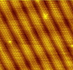
Image of surface reconstruction on a clean Au(100) surface, as visualized using scanning tunneling microscopy. The surface atoms deviate from the bulk crystal structure and arrange in columns several atoms wide with pits between them.
The structure of the Au (100) surface is an interesting example of how a cubic structure can be reconstructed into a different symmetry, as well as the temperature dependence of a reconstruction. In the bulk gold is an (fcc) metal, with a surface structure reconstructed into a distorted hexagonal phase. This hexagonal phase is often referred to as a (28×5) structure, distorted and rotated by about 0.81° relative to the [011] crystal direction. Molecular-dynamics simulations indicate that this rotation occurs to partly relieve a compressive strain developed in the formation of this hexagonal reconstruction, which is nevertheless favored thermodynamically over the unreconstructed structure. However, this rotation disappears in a phase transition at approximately T = 970K, above which an un-rotated hexagonal structure is observed.[10]
A second phase transition is observed at T = 1170K, in which an order–disorder transition occurs, as entropic effects dominate at high temperature. The high-temperature disordered phase is explained as a quasi-melted phase in which only the surface becomes disordered between 1170K and the bulk melting temperature of 1337K. This phase is not completely disordered, however, as this melting process allows the effects of the substrate interactions to become important again in determining the surface structure. This results in a recovery of the square (1×1) structure within the disordered phase and makes sense as at high temperatures the energy reduction allowed by the hexagonal reconstruction can be presumed to be less significant.[10]
↑ Brommer, Karl; Needels, M.; Larson, B.; Joannopoulos, J. (1992). "Ab initio theory of the Si(111)-(7×7) surface reconstruction: A challenge for massively parallel computation". Phys. Rev. Lett. 68 (9): 1355–1359. Bibcode:1992PhRvL..68.1355B. doi:10.1103/PhysRevLett.68.1355. PMID10046145.
Oura, K.; Lifshits, V. G.; Saranin, A. A.; Zotov, A. V.; and Katayama, M. (2003) Surface Science: An Introduction. Berlin: Springer-Verlag. ISBN3-540-00545-5.
This page is based on this Wikipedia article Text is available under the CC BY-SA 4.0 license; additional terms may apply. Images, videos and audio are available under their respective licenses.