
A motherboard is the main printed circuit board (PCB) in general-purpose computers and other expandable systems. It holds and allows communication between many of the crucial electronic components of a system, such as the central processing unit (CPU) and memory, and provides connectors for other peripherals. Unlike a backplane, a motherboard usually contains significant sub-systems, such as the central processor, the chipset's input/output and memory controllers, interface connectors, and other components integrated for general use.

Digital electronics is a field of electronics involving the study of digital signals and the engineering of devices that use or produce them. This is in contrast to analog electronics which work primarily with analog signals. Despite the name, digital electronics designs includes important analog design considerations.

In microelectronics, a dual in-line package is an electronic component package with a rectangular housing and two parallel rows of electrical connecting pins. The package may be through-hole mounted to a printed circuit board (PCB) or inserted in a socket. The dual-inline format was invented by Don Forbes, Rex Rice and Bryant Rogers at Fairchild R&D in 1964, when the restricted number of leads available on circular transistor-style packages became a limitation in the use of integrated circuits. Increasingly complex circuits required more signal and power supply leads ; eventually microprocessors and similar complex devices required more leads than could be put on a DIP package, leading to development of higher-density chip carriers. Furthermore, square and rectangular packages made it easier to route printed-circuit traces beneath the packages.

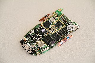
A printed circuit board (PCB), also called printed wiring board (PWB), is a laminated sandwich structure of conductive and insulating layers, each with a pattern of traces, planes and other features etched from one or more sheet layers of copper laminated onto or between sheet layers of a non-conductive substrate. PCBs are used to connect or "wire" components to one another in an electronic circuit. Electrical components may be fixed to conductive pads on the outer layers, generally by soldering, which both electrically connects and mechanically fastens the components to the board. Another manufacturing process adds vias, metal-lined drilled holes that enable electrical interconnections between conductive layers, to boards with more than a single side.

A breadboard, solderless breadboard, or protoboard is a construction base used to build semi-permanent prototypes of electronic circuits. Unlike a perfboard or stripboard, breadboards do not require soldering or destruction of tracks and are hence reusable. For this reason, breadboards are also popular with students and in technological education.

Components of an electrical circuit are electrically connected if an electric current can run between them through an electrical conductor. An electrical connector is an electromechanical device used to create an electrical connection between parts of an electrical circuit, or between different electrical circuits, thereby joining them into a larger circuit.

A ball grid array (BGA) is a type of surface-mount packaging used for integrated circuits. BGA packages are used to permanently mount devices such as microprocessors. A BGA can provide more interconnection pins than can be put on a dual in-line or flat package. The whole bottom surface of the device can be used, instead of just the perimeter. The traces connecting the package's leads to the wires or balls which connect the die to package are also on average shorter than with a perimeter-only type, leading to better performance at high speeds.

Surface-mount technology (SMT), originally called planar mounting, is a method in which the electrical components are mounted directly onto the surface of a printed circuit board (PCB). An electrical component mounted in this manner is referred to as a surface-mount device (SMD). In industry, this approach has largely replaced the through-hole technology construction method of fitting components, in large part because SMT allows for increased manufacturing automation which reduces cost and improves quality. It also allows for more components to fit on a given area of substrate. Both technologies can be used on the same board, with the through-hole technology often used for components not suitable for surface mounting such as large transformers and heat-sinked power semiconductors.

Hot swapping is the replacement or addition of components to a computer system without stopping, shutting down, or rebooting the system; hot plugging describes the addition of components only. Components which have such functionality are said to be hot-swappable or hot-pluggable; likewise, components which do not are cold-swappable or cold-pluggable.
In-circuit emulation (ICE) is the use of a hardware device or in-circuit emulator used to debug the software of an embedded system. It operates by using a processor with the additional ability to support debugging operations, as well as to carry out the main function of the system. Particularly for older systems, with limited processors, this usually involved replacing the processor temporarily with a hardware emulator: a more powerful although more expensive version. It was historically in the form of bond-out processor which has many internal signals brought out for the purpose of debugging. These signals provide information about the state of the processor.

Flip chip, also known as controlled collapse chip connection or its abbreviation, C4, is a method for interconnecting dies such as semiconductor devices, IC chips, integrated passive devices and microelectromechanical systems (MEMS), to external circuitry with solder bumps that have been deposited onto the chip pads. The technique was developed by General Electric's Light Military Electronics Department, Utica, New York. The solder bumps are deposited on the chip pads on the top side of the wafer during the final wafer processing step. In order to mount the chip to external circuitry, it is flipped over so that its top side faces down, and aligned so that its pads align with matching pads on the external circuit, and then the solder is reflowed to complete the interconnect. This is in contrast to wire bonding, in which the chip is mounted upright and fine wires are welded onto the chip pads and lead frame contacts to interconnect the chip pads to external circuitry.

In computer hardware, a CPU socket or CPU slot contains one or more mechanical components providing mechanical and electrical connections between a microprocessor and a printed circuit board (PCB). This allows for placing and replacing the central processing unit (CPU) without soldering.
JTAG is an industry standard for verifying designs of and testing printed circuit boards after manufacture.
In electronics, rework is repair or refinish of a printed circuit board (PCB) assembly, usually involving desoldering and re-soldering of surface-mounted electronic components (SMD). Mass processing techniques are not applicable to single device repair or replacement, and specialized manual techniques by expert personnel using appropriate equipment are required to replace defective components; area array packages such as ball grid array (BGA) devices particularly require expertise and appropriate tools. A hot air gun or hot air station is used to heat devices and melt solder, and specialised tools are used to pick up and position often tiny components. A rework station is a place to do this work—the tools and supplies for this work, typically on a workbench. Other kinds of rework require other tools.
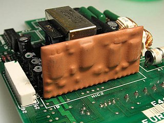
A hybrid integrated circuit (HIC), hybrid microcircuit, hybrid circuit or simply hybrid is a miniaturized electronic circuit constructed of individual devices, such as semiconductor devices and passive components, bonded to a substrate or printed circuit board (PCB). A PCB having components on a Printed wiring board (PWB) is not considered a true hybrid circuit according to the definition of MIL-PRF-38534.

Solder paste is used in the manufacture of printed circuit boards to connect surface mount components to pads on the board. It is also possible to solder through-hole pin in paste components by printing solder paste in and over the holes. The sticky paste temporarily holds components in place; the board is then heated, melting the paste and forming a mechanical bond as well as an electrical connection. The paste is applied to the board by jet printing, stencil printing or syringe; then the components are put in place by a pick-and-place machine or by hand.

Flat no-leads packages such as quad-flat no-leads (QFN) and dual-flat no-leads (DFN) physically and electrically connect integrated circuits to printed circuit boards. Flat no-leads, also known as micro leadframe (MLF) and SON, is a surface-mount technology, one of several package technologies that connect ICs to the surfaces of PCBs without through-holes. Flat no-lead is a near chip scale plastic encapsulated package made with a planar copper lead frame substrate. Perimeter lands on the package bottom provide electrical connections to the PCB. Flat no-lead packages usually, but not always, include an exposed thermally conductive pad to improve heat transfer out of the IC. Heat transfer can be further facilitated by metal vias in the thermal pad. The QFN package is similar to the quad-flat package (QFP), and a ball grid array (BGA).
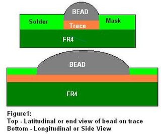
Bead probe technology (BPT) is technique used to provide electrical access to printed circuit board (PCB) circuitry for performing in-circuit testing (ICT). It makes use of small beads of solder placed onto the board's traces to allow measuring and controlling of the signals using a test probe. This permits test access to boards on which standard ICT test pads are not feasible due to space constraints.
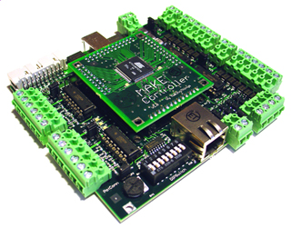
A single-board microcontroller is a microcontroller built onto a single printed circuit board. This board provides all of the circuitry necessary for a useful control task: a microprocessor, I/O circuits, a clock generator, RAM, stored program memory and any necessary support ICs. The intention is that the board is immediately useful to an application developer, without requiring them to spend time and effort to develop controller hardware.

Printed circuit board manufacturing is the process of manufacturing bare printed circuit boards (PCBs) and then populating them with electronic components. It involves the full assembly of a board into a functional circuit board.

