Related Research Articles

Chemical vapor deposition (CVD) is a vacuum deposition method used to produce high-quality, and high-performance, solid materials. The process is often used in the semiconductor industry to produce thin films.
Photolithography is a process used in the manufacturing of integrated circuits. It involves using light to transfer a pattern onto a substrate, typically a silicon wafer.

Semiconductor device fabrication is the process used to manufacture semiconductor devices, typically integrated circuits (ICs) such as microprocessors, microcontrollers, and memories. It is a multiple-step photolithographic and physico-chemical process during which electronic circuits are gradually created on a wafer, typically made of pure single-crystal semiconducting material. Silicon is almost always used, but various compound semiconductors are used for specialized applications.

In electronics, the metal–oxide–semiconductor field-effect transistor is a type of field-effect transistor (FET), most commonly fabricated by the controlled oxidation of silicon. It has an insulated gate, the voltage of which determines the conductivity of the device. This ability to change conductivity with the amount of applied voltage can be used for amplifying or switching electronic signals. The term metal–insulator–semiconductor field-effect transistor (MISFET) is almost synonymous with MOSFET. Another near-synonym is insulated-gate field-effect transistor (IGFET).

Complementary metal–oxide–semiconductor is a type of metal–oxide–semiconductor field-effect transistor (MOSFET) fabrication process that uses complementary and symmetrical pairs of p-type and n-type MOSFETs for logic functions. CMOS technology is used for constructing integrated circuit (IC) chips, including microprocessors, microcontrollers, memory chips, and other digital logic circuits. CMOS technology is also used for analog circuits such as image sensors, data converters, RF circuits, and highly integrated transceivers for many types of communication.

Flip chip, also known as controlled collapse chip connection or its abbreviation, C4, is a method for interconnecting dies such as semiconductor devices, IC chips, integrated passive devices and microelectromechanical systems (MEMS), to external circuitry with solder bumps that have been deposited onto the chip pads. The technique was developed by General Electric's Light Military Electronics Department, Utica, New York. The solder bumps are deposited on the chip pads on the top side of the wafer during the final wafer processing step. In order to mount the chip to external circuitry, it is flipped over so that its top side faces down, and aligned so that its pads align with matching pads on the external circuit, and then the solder is reflowed to complete the interconnect. This is in contrast to wire bonding, in which the chip is mounted upright and fine wires are welded onto the chip pads and lead frame contacts to interconnect the chip pads to external circuitry.
Fused quartz, fused silica or quartz glass is a glass consisting of almost pure silica (silicon dioxide, SiO2) in amorphous (non-crystalline) form. This differs from all other commercial glasses, such as soda-lime glass, lead glass, or borosilicate glass, in which other ingredients are added which change the glasses' optical and physical properties, such as lowering the melt temperature, the spectral transmission range, or the mechanical strength. Fused quartz, therefore, has high working and melting temperatures, making it difficult to form and less desirable for most common applications, but is much stronger, more chemically resistant, and exhibits lower thermal expansion, making it more suitable for many specialized uses such as lighting and scientific applications.
In semiconductor manufacturing, silicon on insulator (SOI) technology is fabrication of silicon semiconductor devices in a layered silicon–insulator–silicon substrate, to reduce parasitic capacitance within the device, thereby improving performance. SOI-based devices differ from conventional silicon-built devices in that the silicon junction is above an electrical insulator, typically silicon dioxide or sapphire. The choice of insulator depends largely on intended application, with sapphire being used for high-performance radio frequency (RF) and radiation-sensitive applications, and silicon dioxide for diminished short-channel effects in other microelectronics devices. The insulating layer and topmost silicon layer also vary widely with application.
In semiconductor manufacturing, a low-κ is a material with a small relative dielectric constant relative to silicon dioxide. Low-κ dielectric material implementation is one of several strategies used to allow continued scaling of microelectronic devices, colloquially referred to as extending Moore's law. In digital circuits, insulating dielectrics separate the conducting parts from one another. As components have scaled and transistors have gotten closer together, the insulating dielectrics have thinned to the point where charge build up and crosstalk adversely affect the performance of the device. Replacing the silicon dioxide with a low-κ dielectric of the same thickness reduces parasitic capacitance, enabling faster switching speeds and lower heat dissipation. In conversation such materials may be referred to as "low-k" rather than "low-κ" (low-kappa).
Aluminium nitride (AlN) is a solid nitride of aluminium. It has a high thermal conductivity of up to 321 W/(m·K) and is an electrical insulator. Its wurtzite phase (w-AlN) has a band gap of ~6 eV at room temperature and has a potential application in optoelectronics operating at deep ultraviolet frequencies.

The planar process is a manufacturing process used in the semiconductor industry to build individual components of a transistor, and in turn, connect those transistors together. It is the primary process by which silicon integrated circuit chips are built, and it is the most commonly used method of producing junctions during the manufacture of semiconductor devices. The process utilizes the surface passivation and thermal oxidation methods.
An organic field-effect transistor (OFET) is a field-effect transistor using an organic semiconductor in its channel. OFETs can be prepared either by vacuum evaporation of small molecules, by solution-casting of polymers or small molecules, or by mechanical transfer of a peeled single-crystalline organic layer onto a substrate. These devices have been developed to realize low-cost, large-area electronic products and biodegradable electronics. OFETs have been fabricated with various device geometries. The most commonly used device geometry is bottom gate with top drain and source electrodes, because this geometry is similar to the thin-film silicon transistor (TFT) using thermally grown SiO2 as gate dielectric. Organic polymers, such as poly(methyl-methacrylate) (PMMA), can also be used as dielectric. One of the benefits of OFETs, especially compared with inorganic TFTs, is their unprecedented physical flexibility, which leads to biocompatible applications, for instance in the future health care industry of personalized biomedicines and bioelectronics.
The 65 nm process is an advanced lithographic node used in volume CMOS (MOSFET) semiconductor fabrication. Printed linewidths can reach as low as 25 nm on a nominally 65 nm process, while the pitch between two lines may be greater than 130 nm.
In semiconductor fabrication, a resist is a thin layer used to transfer a circuit pattern to the semiconductor substrate which it is deposited upon. A resist can be patterned via lithography to form a (sub)micrometer-scale, temporary mask that protects selected areas of the underlying substrate during subsequent processing steps. The material used to prepare said thin layer is typically a viscous solution. Resists are generally proprietary mixtures of a polymer or its precursor and other small molecules that have been specially formulated for a given lithography technology. Resists used during photolithography are called photoresists.
In the semiconductor industry, the term high-κ dielectric refers to a material with a high dielectric constant, as compared to silicon dioxide. High-κ dielectrics are used in semiconductor manufacturing processes where they are usually used to replace a silicon dioxide gate dielectric or another dielectric layer of a device. The implementation of high-κ gate dielectrics is one of several strategies developed to allow further miniaturization of microelectronic components, colloquially referred to as extending Moore's Law.
Lam Research Corporation is an American supplier of wafer-fabrication equipment and related services to the semiconductor industry. Its products are used primarily in front-end wafer processing, which involves the steps that create the active components of semiconductor devices and their wiring (interconnects). The company also builds equipment for back-end wafer-level packaging (WLP) and for related manufacturing markets such as for microelectromechanical systems (MEMS).
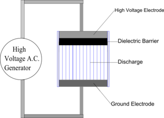
Dielectric-barrier discharge (DBD) is the electrical discharge between two electrodes separated by an insulating dielectric barrier. Originally called silent (inaudible) discharge and also known as ozone production discharge or partial discharge, it was first reported by Ernst Werner von Siemens in 1857.
Resistive random-access memory is a type of non-volatile (NV) random-access (RAM) computer memory that works by changing the resistance across a dielectric solid-state material, often referred to as a memristor. One major advantage of ReRAM over other NVRAM technologies is the ability to scale below 10 nm.
Thermally stimulated current (TSC) spectroscopy is an experimental technique which is used to study energy levels in semiconductors or insulators. Energy levels are first filled either by optical or electrical injection usually at a relatively low temperature, subsequently electrons or holes are emitted by heating to a higher temperature. A curve of emitted current will be recorded and plotted against temperature, resulting in a TSC spectrum. By analyzing TSC spectra, information can be obtained regarding energy levels in semiconductors or insulators.
A semiconductor package is a metal, plastic, glass, or ceramic casing containing one or more discrete semiconductor devices or integrated circuits. Individual components are fabricated on semiconductor wafers before being diced into die, tested, and packaged. The package provides a means for connecting it to the external environment, such as printed circuit board, via leads such as lands, balls, or pins; and protection against threats such as mechanical impact, chemical contamination, and light exposure. Additionally, it helps dissipate heat produced by the device, with or without the aid of a heat spreader. There are thousands of package types in use. Some are defined by international, national, or industry standards, while others are particular to an individual manufacturer.
References
- ↑ Gupta, Nishant (December 2012). "Photo-thermal Processing of Semiconductor Fibers and Thin Films". All Dissertations. clemson.edu. Bibcode:2012PhDT.......211G . Retrieved 2016-05-03.
- ↑ Singh, R.; Cherukuri, K. C.; Vedula, L.; Rohatgi, A.; Narayanan, S. (1996-05-13). "Low temperature shallow junction formation using vacuum ultraviolet photons during rapid thermal processing". Applied Physics Letters. 70 (13). scitation.aip.org: 1700–1702. doi:10.1063/1.118674.
- ↑ Rapid Thermal Processing for Future Semiconductor Devices. Elsevier Science B.V. 2003-04-02. ISBN 9780080540269 . Retrieved 2016-05-04.
| | This industry-related article is a stub. You can help Wikipedia by expanding it. |