Wright etch

Last updated
Margaret Wright Jenkins; 1936-2018 Margaret Wright Jenkins 2014.jpg
Margaret Wright Jenkins; 1936–2018

The Wright etch (also Wright-Jenkins etch) is a preferential etch for revealing defects in <100>- and <111>-oriented, p- and n-type silicon wafers used for making transistors, microprocessors, memories, and other components. Revealing, identifying, and remedying such defects is essential for progress along the path predicted by Moore's law. It was developed by Margaret Wright Jenkins (1936-2018) in 1976 while working in research and development at Motorola Inc. in Phoenix, AZ. It was published in 1977. [1] This etchant reveals clearly defined oxidation-induced stacking faults, dislocations, swirls and striations with minimum surface roughness or extraneous pitting. These defects are known causes of shorts and current leakage in finished semiconductor devices (such as transistors) should they fall across isolated junctions. A relatively low etch rate (~1 micrometre per minute) at room temperature provides etch control. The long shelf life of this etchant allows the solution to be stored in large quantities. [1]

Contents

Etch formula

The composition of the Wright etch is as follows:

In mixing the solution, the best results are obtained by first dissolving the copper nitrate in the given amount of water; otherwise the order of mixing is not critical.

Etch mechanism

The Wright etch consistently produces well-defined etch figures of common defects on silicon surfaces. This effect is attributed to the interactions of the selected chemicals in the formula. Robbins and Schwartz [2] [3] [4] described chemical etching of silicon in detail using an HF, HNO3 and H2O system; and an HF, HNO3, H2O and CH3COOH (acetic acid) system. Briefly, the etching of silicon is a two-step process. First, the top surface of the silicon is converted into a soluble oxide by a suitable oxidizing agent(s). Then the resulting oxide layer is removed from the surface by dissolution in a suitable solvent, usually HF. This is a continuous process during the etch cycle. In order to delineate a crystal defect, the defect area must be oxidized at a slower or faster rate than the surrounding area thereby forming a mound or pit during the preferential etch process.

In the present system, the silicon is oxidized with HNO3, CrO3 solution (which in this case contains the Cr2O72− dichromate ion, since the pH is low - see the phase diagram in chromic acid) and Cu (NO3)2. The dichromate ion, a strong oxidizing agent, is considered to be the principal oxidizing agent. The ratio of HNO3 to CrO3 solution stated in the formula produces a superior etched surface. Other ratios produce less desirable finishes. With the addition of a small amount of Cu (NO3)2, the definition of the defect was enhanced. Therefore, it is believed that the Cu (NO3)2 affects the localized differential oxidation rate at the defect site. The addition of the acetic acid gave the background surface of the etched silicon a smooth finish. It is theorized that this effect is attributed to the wetting action of the acetic acid which prevents the formation of bubbles during etching.

All experimental preferential etching to show defects was done on cleaned and oxidized wafers. All oxidations were performed at 1200 °C in steam for 75 minutes. Figure 1 (a) shows oxidation-induced stacking faults in <100>-oriented wafers after 30 minutes Wright etch, (b) and (c) show dislocation pits on <100>- and <111>-oriented wafers respectively after 20 minutes Wright etch. [1]

Figure 1 (a),(b),(c) Fig1a.b.c.jpg
Figure 1 (a),(b),(c)

Figure 1 (a) shows oxidation-induced stacking faults on a <100>-oriented, 7-10 Ω-cm, boron-doped wafer after 30 minutes Wright etch (the A arrow in this figure points to the shape of faults that intersect the surface, while B points to bulk faults). Figure 1 (b) and (c) show dislocation pits on <100>- and <111>-oriented wafers respectively after 20 minutes Wright etch. [1]

Summary

This etch process is a quick and reliable method of determining the integrity of pre-processed polished silicon wafers or to reveal defects that may be induced at any point during wafer processing. It has been demonstrated that Wright etch is superior in revealing stacking faults and dislocation etch figures when compared with those revealed by Sirtl [5] and Secco etchings. [6]

This etch is widely used in failure analysis of electrical devices at various wafer processing stages. [7] [8] In comparison, the Wright etch was often the preferred etchant to reveal defects in silicon crystals. [7] [8]

Figure 2 (a),(b),(c): Wright etch comparison micrographs Wright.Etch.Fig2a.b.c.jpg
Figure 2 (a),(b),(c): Wright etch comparison micrographs

Figure 2 shows a comparison of oxidation-induced stacking fault delineation on <100>-oriented wafers after Wright etch, Secco and Sirtl etch respectively. [1]

Figure 3 shows a comparison of dislocation pits delineation on <100>-oriented wafers after Wright etch, Secco and Sirtl etch. The final figure 4 shows a comparison of dislocation pits revealed on a <111>-oriented wafer after etching with Wright etch, Secco and Sirtl etch respectively. [1]

Figure 3 (a),(b),(c): Wright etch comparison micrographs Wright.Etch.Fig3a.b.c.jpg
Figure 3 (a),(b),(c): Wright etch comparison micrographs

Figure 3 shows a comparison of dislocation delineation on a <100>-oriented, 10-20 Ω-cm, boron doped wafer after oxidation and preferential etching. (a) After 20 minutes Wright etch, (b) 10 minutes Secco etch and (c) 6 minutes Sirtl etch. [1]

Figure 4 (a),(b),(c): Wright etch comparison micrographs Wright.Etch.Fig4a.b.c.jpg
Figure 4 (a),(b),(c): Wright etch comparison micrographs

Figure 4 shows a comparison of dislocation delineation on a <111>-oriented, 10-20 Ω-cm, boron-doped wafer after oxidation and preferential etching. (a) After 10 minutes Wright etch, (b) 10 minutes Secco etch and (c) 3 minutes Sirtl etch. The arrows indicate slip direction. [1]

Related Research Articles

<span class="mw-page-title-main">MEMS</span> Very small devices that incorporate moving components

MEMS is the technology of microscopic devices incorporating both electronic and moving parts. MEMS are made up of components between 1 and 100 micrometres in size, and MEMS devices generally range in size from 20 micrometres to a millimetre, although components arranged in arrays can be more than 1000 mm2. They usually consist of a central unit that processes data and several components that interact with the surroundings.

<span class="mw-page-title-main">Nitric acid</span> Highly corrosive mineral acid

Nitric acid is an inorganic compound with the formula HNO3. It is a highly corrosive mineral acid. The compound is colorless, but samples tend to acquire a yellow cast over time due to decomposition into oxides of nitrogen. Most commercially available nitric acid has a concentration of 68% in water. When the solution contains more than 86% HNO3, it is referred to as fuming nitric acid. Depending on the amount of nitrogen dioxide present, fuming nitric acid is further characterized as red fuming nitric acid at concentrations above 86%, or white fuming nitric acid at concentrations above 95%.

<span class="mw-page-title-main">Semiconductor device fabrication</span> Manufacturing process used to create integrated circuits

Semiconductor device fabrication is the process used to manufacture semiconductor devices, typically integrated circuits (ICs) such as microprocessors, microcontrollers, and memories. It is a multiple-step photolithographic and physico-chemical process during which electronic circuits are gradually created on a wafer, typically made of pure single-crystal semiconducting material. Silicon is almost always used, but various compound semiconductors are used for specialized applications.

<span class="mw-page-title-main">Red fuming nitric acid</span> Chemical compound

Red fuming nitric acid (RFNA) is a storable oxidizer used as a rocket propellant. It consists of 84% nitric acid, 13% dinitrogen tetroxide and 1–2% water. The color of red fuming nitric acid is due to the dinitrogen tetroxide, which breaks down partially to form nitrogen dioxide. The nitrogen dioxide dissolves until the liquid is saturated, and produces toxic fumes with a suffocating odor. RFNA increases the flammability of combustible materials and is highly exothermic when reacting with water.

<span class="mw-page-title-main">Hydrofluoric acid</span> Solution of hydrogen fluoride in water

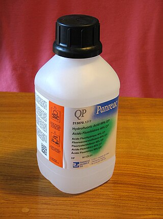
Hydrofluoric acid is a solution of hydrogen fluoride (HF) in water. Solutions of HF are colorless, acidic and highly corrosive. A common concentration is 49% (48-52%) but there are also stronger solutions and pure HF has a boiling point near room temperature. It is used to make most fluorine-containing compounds; examples include the commonly used pharmaceutical antidepressant medication fluoxetine (Prozac) and the material PTFE (Teflon). Elemental fluorine is produced from it. It is commonly used to etch glass and silicon wafers.

<span class="mw-page-title-main">Ceric ammonium nitrate</span> Chemical compound

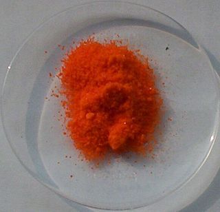
Ceric ammonium nitrate (CAN) is the inorganic compound with the formula (NH4)2[Ce(NO3)6]. This orange-red, water-soluble cerium salt is a specialised oxidizing agent in organic synthesis and a standard oxidant in quantitative analysis.

<span class="mw-page-title-main">Planar process</span> Process used to make microchips

The planar process is a manufacturing process used in the semiconductor industry to build individual components of a transistor, and in turn, connect those transistors together. It is the primary process by which silicon integrated circuit chips are built, and it is the most commonly used method of producing junctions during the manufacture of semiconductor devices. The process utilizes the surface passivation and thermal oxidation methods.

Chemical mechanical polishing (CMP) is a process of smoothing surfaces with the combination of chemical and mechanical forces. It can be thought of as a hybrid of chemical etching and free abrasive polishing. It is used in the semiconductor industry to polish semiconductor wafers as part of the integrated circuit manufacturing process.

<span class="mw-page-title-main">Ammonium fluoride</span> Chemical compound

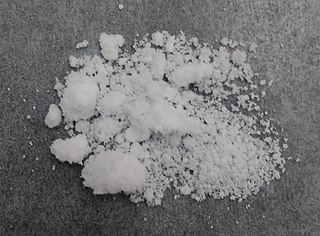
Ammonium fluoride is the inorganic compound with the formula NH4F. It crystallizes as small colourless prisms, having a sharp saline taste, and is highly soluble in water. Like all fluoride salts, it is moderately toxic in both acute and chronic overdose.

<span class="mw-page-title-main">Lead dioxide</span> Chemical compound

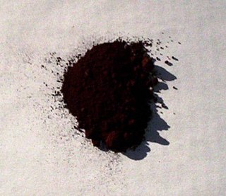
Lead(IV) oxide, commonly known as lead dioxide, is an inorganic compound with the chemical formula PbO2. It is an oxide where lead is in an oxidation state of +4. It is a dark-brown solid which is insoluble in water. It exists in two crystalline forms. It has several important applications in electrochemistry, in particular as the positive plate of lead acid batteries.

Porous silicon is a form of the chemical element silicon that has introduced nanopores in its microstructure, rendering a large surface to volume ratio in the order of 500 m2/cm3.

The etch pit density (EPD) is a measure for the quality of semiconductor wafers.

<span class="mw-page-title-main">Piranha solution</span> Oxidizing acid mixture containing sulfuric acid and hydrogen peroxide

Piranha solution, also known as piranha etch, is a mixture of sulfuric acid and hydrogen peroxide. The resulting mixture is used to clean organic residues off substrates, for example silicon wafers. Because the mixture is a strong oxidizing agent, it will decompose most organic matter, and it will also hydroxylate most surfaces, making them highly hydrophilic (water-compatible). This means the solution can also easily dissolve fabric and skin, potentially causing severe damage and chemical burns in case of inadvertent contact. It is named after the piranha fish due to its tendency to rapidly dissolve and 'consume' organic materials through vigorous chemical reactions.

The RCA clean is a standard set of wafer cleaning steps which need to be performed before high-temperature processing steps of silicon wafers in semiconductor manufacturing.

<span class="mw-page-title-main">Etching (microfabrication)</span> Technique in microfabrication used to remove material and create structures

Etching is used in microfabrication to chemically remove layers from the surface of a wafer during manufacturing. Etching is a critically important process module in fabrication, and every wafer undergoes many etching steps before it is complete.

Plasma-activated bonding is a derivative, directed to lower processing temperatures for direct bonding with hydrophilic surfaces. The main requirements for lowering temperatures of direct bonding are the use of materials melting at low temperatures and with different coefficients of thermal expansion (CTE).

<span class="mw-page-title-main">Chemistry of photolithography</span> Overview article

Photolithography is a process in removing select portions of thin films used in microfabrication. Microfabrication is the production of parts on the micro- and nano- scale, typically on the surface of silicon wafers, for the production of integrated circuits, microelectromechanical systems (MEMS), solar cells, and other devices. Photolithography makes this process possible through the combined use of hexamethyldisilazane (HMDS), photoresist, spin coating, photomask, an exposure system and other various chemicals. By carefully manipulating these factors it is possible to create nearly any geometry microstructure on the surface of a silicon wafer. The chemical interaction between all the different components and the surface of the silicon wafer makes photolithography an interesting chemistry problem. Current engineering has been able to create features on the surface of silicon wafers between 1 and 100 μm.

<span class="mw-page-title-main">Zirconium nitrate</span> Chemical compound

Zirconium nitrate is a volatile anhydrous transition metal nitrate salt of zirconium with formula Zr(NO3)4. It has alternate names of zirconium tetranitrate, or zirconium(IV) nitrate.

<span class="mw-page-title-main">Metal assisted chemical etching</span>

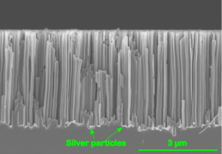
Metal Assisted Chemical Etching is the process of wet chemical etching of semiconductors with the use of a metal catalyst, usually deposited on the surface of a semiconductor in the form of a thin film or nanoparticles. The semiconductor, covered with the metal is then immersed in an etching solution containing and oxidizing agent and hydrofluoric acid. The metal on the surface catalyzes the reduction of the oxidizing agent and therefore in turn also the dissolution of silicon. In the majority of the conducted research this phenomenon of increased dissolution rate is also spatially confined, such that it is increased in close proximity to a metal particle at the surface. Eventually this leads to the formation of straight pores that are etched into the semiconductor. This means that a pre-defined pattern of the metal on the surface can be directly transferred to a semiconductor substrate.

Vapor etching refers to a process used in the fabrication of Microelectromechanical systems (MEMS) and Nanoelectromechanical systems (NEMS). Sacrificial layers are isotropically etched using gaseous acids such as Hydrogen fluoride and Xenon difluoride to release the free standing components of the device.

References

  1. 1 2 3 4 5 6 7 8 9 10 11 12 Wright Jenkins, Margaret (1977). "A New Preferential Etch for Defects in Silicon Crystals". Journal of the Electrochemical Society . 124 (5): 757–759. Bibcode:1977JElS..124..757W. doi:10.1149/1.2133401 . Retrieved 2019-04-06.
  2. Robbins, Harry; Schwartz, Bertram (1959). "Chemical Etching of Silicon: Part I. The System HF, HNO3, and H2O". Journal of the Electrochemical Society . 106 (6): 505–508. doi:10.1149/1.2427397.
  3. Robbins, Harry; Schwartz, Bertram (1960). "Chemical Etching of Silicon: Part II. The System HF, HNO3, H2O, and HC2H3O2". Journal of the Electrochemical Society . 107 (2): 108–111. doi:10.1149/1.2427617.
  4. Robbins, Harry; Schwartz, Bertram (1961). "Chemical Etching of Silicon: Part III. A Temperature Study in the Acid System". Journal of the Electrochemical Society . 108 (4): 365–372. doi:10.1149/1.2428090.
  5. Sirtl, Erhard; Adler, Annemarie (1961). "Chromsäure-Flussäure als Spezifisches System zur Ätzgrubenentwicklung auf Silizium". Zeitschrift für Metallkunde (in German). 52 (8): 529–534. NAID   10011334657.
  6. Secco d'Aragona, F. (1972). "Dislocation Etch for (100) Planes in Silicon". Journal of the Electrochemical Society . 119 (7): 948–951. Bibcode:1972JElS..119..948S. doi:10.1149/1.2404374.
  7. 1 2 Su, Garth K.; Jin, Da; Kim, Sung-Rae; Chan, Tze-Ho; Balan, Hari; Lin, Yung-Tao; Han, Kyung-Joon; Hsia, Steve (2003). "CMOS: Defect Avoidance - Pipeline Defects in Flash Devices Associated with Rings OSF" (PDF). Semiconductor Manufacturing: 144–151. Archived from the original (PDF) on 2016-03-03. Retrieved 2019-04-06.
  8. 1 2 "Chapter 6". Defect Etching in Silicon. 2002. Archived from the original on 2019-04-06. Retrieved 2019-04-06.