Carbon nanotube field-effect transistor

Last updated

A carbon nanotube field-effect transistor (CNTFET) is a field-effect transistor that utilizes a single carbon nanotube (CNT) or an array of carbon nanotubes as the channel material, instead of bulk silicon, as in the traditional MOSFET structure. There have been major developments since CNTFETs were first demonstrated in 1998. [1] [2]

Contents

Background

A diagram showing that a carbon nanotube is essentially rolled up graphene Roll-up.jpg
A diagram showing that a carbon nanotube is essentially rolled up graphene

According to Moore's law, the dimensions of individual devices in an integrated circuit have been decreased by a factor of approximately two every two years. This scaling down of devices has been the driving force in technological advances since the late 20th century. However, as noted by ITRS 2009 edition, further scaling down has faced serious limits related to fabrication technology and device performances as the critical dimension shrunk down to sub-22 nm range. [3] The limits involve electron tunneling through short channels and thin insulator films, the associated leakage currents, passive power dissipation, short channel effects, and variations in device structure and doping. [4] These limits can be overcome to some extent and facilitate further scaling down of device dimensions by modifying the channel material in the traditional bulk MOSFET structure with a single carbon nanotube or an array of carbon nanotubes.

A carbon nanotube’s bandgap is directly affected by its chiral angle and diameter. If those properties can be controlled, CNTs would be a promising candidate for future nano-scale transistor devices. Moreover, because of the lack of boundaries in the perfect and hollow cylinder structure of CNTs, there is no boundary scattering. CNTs are also quasi-1D materials in which only forward scattering and back scattering are allowed, and elastic scattering means that free paths in carbon nanotubes are long, typically on the order of micrometers. As a result, quasi-ballistic transport can be observed in nanotubes at relatively long lengths and low fields. [5] Because of the strong covalent carbon–carbon bonding in the sp2 configuration, carbon nanotubes are chemically inert and are able to transport large electric currents. In theory, carbon nanotubes are also able to conduct heat nearly as well as diamond or sapphire, and because of their miniaturized dimensions, the CNTFET should switch reliably using much less power than a silicon-based device. [6]

Electronic structure of carbon nanotubes

Graphene atomic structure with a translational vector T and a chiral vector Ch of a CNT Chiral vector.jpg
Graphene atomic structure with a translational vector T and a chiral vector Ĉh of a CNT
One-dimensional energy dispersion relations for (a) (n,m)=(5,5) metallic tube, (b) (n,m)=(10,0) semiconducting tube. Cntdispersion.jpg
One-dimensional energy dispersion relations for (a) (n,m)=(5,5) metallic tube, (b) (n,m)=(10,0) semiconducting tube.

To a first approximation, the exceptional electrical properties of carbon nanotubes can be viewed as inherited from the unique electronic structure of graphene, provided the carbon nanotube is thought of as graphene rolled up along one of its Bravais lattice vectors Ĉh to form a hollow cylinder. [7] [8] [9] In this construction, periodic boundary conditions are imposed over Ĉh to yield a lattice of seamlessly bonded carbon atoms on the cylinder surface. [10]

Thus, the circumference of such a carbon nanotube can be expressed in terms of its rollup vector: Ĉh=nâ1+mâ2 that connects two crystallographically equivalent sites of the two-dimensional graphene sheet. Here and are integers and â1 and â2 are primitive lattice vectors of the hexagonal lattice. Therefore, the structure of any carbon nanotube can be described by an index with a pair of integers that define its rollup vector. [8] In terms of the integers , the nanotube diameter and the chiral angle are given by: ; and, , where is the C—C bond distance.

Differences in the chiral angle and the diameter cause the differences in the properties of the various carbon nanotubes. For example, it can be shown that an carbon nanotube is metallic when , [7] is a small band gap semiconductor when and , [8] [9] and is a moderate band gap semiconductor when , [8] [9] where is an integer.

These results can be motivated by noting that periodic boundary conditions for 1D carbon nanotubes permit only a few wave vectors to exist around their circumferences. Metallic conduction could be expected to occur when one of these wave vectors passes through the K-point of graphene’s 2D hexagonal Brillouin zone, where the valence and conduction bands are degenerate.

This analysis, however, neglects the effects of curvature caused by rolling up the graphene sheet that converts all nanotubes with to small band gap semiconductors, [8] [9] with the exception of the armchair tubes () that remain metallic. [7] Although the band gaps of carbon nanotubes with and are relatively small, some can still easily exceed room temperature, if the nanotube diameter is about a nanometer. [11] [12]

The band gaps of semiconducting carbon nanotubes with depend predominately on their diameters. In fact, according to a single-particle tight-binding description of the electronic structure of these nanotubes [13] where is the nearest-neighbor hopping matrix element. That this result is an excellent approximation so long as is a lot less than one has been verified both by all-electron first principles local density functional calculations [14] and experiment. [15]

Scatter plots of the band gaps of carbon nanotubes with diameters up to three nanometers calculated using an all valence tight binding model that includes curvature effects appeared early in carbon nanotube research [11] and were reprinted in a review. [16]

Device fabrication

There are many types of CNTFET devices; a general survey of the most common geometries are covered below.

Back-gated CNTFETs

CNT-FET diagram top.jpg
Top view
CNT-FET diagram side.jpg
Side view
Top and side view of a silicon back-gated CNTFET. The CNTFET consists of carbon nanotubes deposited on a silicon oxide substrate pre-patterned with chromium/gold source and drain contacts.

The earliest techniques for fabricating carbon nanotube (CNT) field-effect transistors involved pre-patterning parallel strips of metal across a silicon dioxide substrate, and then depositing the CNTs on top in a random pattern. [1] [2] The semiconducting CNTs that happened to fall across two metal strips meet all the requirements necessary for a rudimentary field-effect transistor. One metal strip is the "source" contact while the other is the "drain" contact. The silicon oxide substrate can be used as the gate oxide and adding a metal contact on the back makes the semiconducting CNT gateable.

This technique suffered from several drawbacks, which made for non-optimized transistors. The first was the metal contact, which actually had very little contact to the CNT, since the nanotube just lay on top of it and the contact area was therefore very small. Also, due to the semiconducting nature of the CNT, a Schottky barrier forms at the metal–semiconductor interface, [17] increasing the contact resistance. The second drawback was due to the back-gate device geometry. Its thickness made it difficult to switch the devices on and off using low voltages, and the fabrication process led to poor contact between the gate dielectric and CNT. [18]

Top-gated CNTFETs

The process for fabricating a top-gated CNTFET. CNTFET Topgate Fab.jpg
The process for fabricating a top-gated CNTFET.

Eventually, researchers migrated from the back-gate approach to a more advanced top-gate fabrication process. [18] In the first step, single-walled carbon nanotubes are solution deposited onto a silicon oxide substrate. Individual nanotubes are then located via atomic force microscope or scanning electron microscope. After an individual tube is isolated, source and drain contacts are defined and patterned using high resolution electron beam lithography. A high temperature anneal step reduces the contact resistance by improving adhesion between the contacts and CNT. [19] A thin top-gate dielectric is then deposited on top of the nanotube, either via evaporation or atomic layer deposition. Finally, the top gate contact is deposited on the gate dielectric, completing the process.

Arrays of top-gated CNTFETs can be fabricated on the same wafer, since the gate contacts are electrically isolated from each other, unlike in the back-gated case. Also, due to the thinness of the gate dielectric, a larger electric field can be generated with respect to the nanotube using a lower gate voltage. These advantages mean top-gated devices are generally preferred over back-gated CNTFETs, despite their more complex fabrication process.

Wrap-around gate CNTFETs

CNT Sheathed.jpg
Sheathed CNT
WraparoundCNTFET.jpg
Gate all-around CNT Device

Wrap-around gate CNTFETs, also known as gate-all-around CNTFETs were developed in 2008, [20] and are a further improvement upon the top-gate device geometry. In this device, instead of gating just the part of the CNT that is closer to the metal gate contact, the entire circumference of the nanotube is gated. This should ideally improve the electrical performance of the CNTFET, reducing leakage current and improving the device on/off ratio.

Device fabrication begins by first wrapping CNTs in a gate dielectric and gate contact via atomic layer deposition. [21] These wrapped nanotubes are then solution-deposited on an insulating substrate, where the wrappings are partially etched off, exposing the ends of the nanotube. The source, drain, and gate contacts are then deposited onto the CNT ends and the metallic outer gate wrapping.

Suspended CNTFETs

A suspended CNTFET device. Wiki6.jpg
A suspended CNTFET device.

Yet another CNTFET device geometry involves suspending the nanotube over a trench to reduce contact with the substrate and gate oxide. [22] This technique has the advantage of reduced scattering at the CNT-substrate interface, improving device performance. [22] [23] [24] There are many methods used to fabricate suspended CNTFETs, ranging from growing them over trenches using catalyst particles, [22] transferring them onto a substrate and then under-etching the dielectric beneath, [24] and transfer-printing onto a trenched substrate. [23]

The main problem suffered by suspended CNTFETs is that they have very limited material options for use as a gate dielectric (generally air or vacuum), and applying a gate bias has the effect of pulling the nanotube closer to the gate, which places an upper limit on how much the nanotube can be gated. This technique will also only work for shorter nanotubes, as longer tubes will flex in the middle and droop towards the gate, possibly touching the metal contact and shorting the device. In general, suspended CNTFETs are not practical for commercial applications, but they can be useful for studying the intrinsic properties of clean nanotubes.

CNTFET material considerations

There are general decisions one must make when considering what materials to use when fabricating a CNTFET. Semiconducting single-walled carbon nanotubes are preferred over metallic single-walled and metallic multi-walled tubes since they are able to be fully switched off, at least for low source/drain biases. A lot of work has been put into finding a suitable contact material for semiconducting CNTs; the best material to date is Palladium, because its work function closely matches that of nanotubes and it adheres to the CNTs quite well. [25]

Characteristics

Field effect mobility of a back-gated CNTFET device with varying channel lengths. SiO2 is used as the gate dielectric. Tool: 'CNT Mobility' at nanoHUB.org Cntfet.gif
Field effect mobility of a back-gated CNTFET device with varying channel lengths. SiO2 is used as the gate dielectric. Tool: 'CNT Mobility' at nanoHUB.org

In CNT–metal contacts, the different work functions of the metal and the CNT result in a Schottky barrier at the source and drain, which are made of metals like silver, titanium, palladium and aluminum. [27] Even though like Schottky barrier diodes, the barriers would have made this FET to transport only one type of carrier, the carrier transport through the metal-CNT interface is dominated by quantum mechanical tunneling through the Schottky barrier. CNTFETs can easily be thinned by the gate field such that tunneling through them results in a substantial current contribution. CNTFETs are ambipolar; either electrons or holes, or both electrons and holes can be injected simultaneously. [27] This makes the thickness of the Schottky barrier a critical factor.

CNTFETs conduct electrons when a positive bias is applied to the gate and holes when a negative bias is applied, and drain current increases with increasing a magnitude of an applied gate voltage. [28] Around Vg = Vds/2, the current gets the minimum due to the same amount of the electron and hole contributions to the current.

Like other FETs, the drain current increases with an increasing drain bias unless the applied gate voltage is below the threshold voltage. For planar CNTFETs with different design parameters, the FET with a shorter channel length produces a higher saturation current, and the saturation drain current also becomes higher for the FET consisting of smaller diameter keeping the length constant. For cylindrical CNTFETs, it is clear that a higher drain current is driven than that of planar CNTFETs since a CNT is surrounded by an oxide layer which is finally surrounded by a metal contact serving as the gate terminal. [29]

Theoretical derivation of drain current

Structure of a top-gate CNT transistor Cntfet.png
Structure of a top-gate CNT transistor

Theoretical investigation on drain current of the top-gate CNT transistor has been done by Kazierski and colleagues. [30] When an electric field is applied to a CNT transistor, a mobile charge is induced in the tube from the source and drain. These charges are from the density of positive velocity states filled by the source NS and that of negative velocity states filled by the drain ND, [30] and these densities are determined by the Fermi–Dirac probability distributions.

and the equilibrium electron density is

.

where the density of states at the channel D(E), USF, and UDF are defined as

The term, is 1 when the value inside the bracket is positive and 0 when negative. VSC is the self-consistent voltage that illustrates that the CNT energy is affected by external terminal voltages and is implicitly related to the device terminal voltages and charges at terminal capacitances by the following nonlinear equation:

where Qt represents the charge stored in terminal capacitances, and the total terminal capacitance CΣ is the sum of the gate, drain, source, and substrate capacitances shown in the figure above. The standard approach to the solution to the self-consistent voltage equation is to use the Newton–Raphson iterative method. According to the CNT ballistic transport theory, the drain current caused by the transport of the nonequilibrium charge across the nanotube can be calculated using the Fermi–Dirac statistics.

Here F0 represents the Fermi–Dirac integral of order 0, k is the Boltzmann constant, T is the temperature, and ℏ the reduced Planck constant. This equation can be solved easily as long as the self-consistent voltage is known. However the calculation could be time-consuming when it needs to solve the self-consistent voltage with the iterative method, and this is the main drawback of this calculation.

Heat dissipation

The decrease of the current and burning of the CNT can occur due to the temperature raised by several hundreds of kelvins. Generally, the self-heating effect is much less severe in a semiconducting CNTFET than in a metallic one due to different heat dissipation mechanisms. A small fraction of the heat generated in the CNTFET is dissipated through the channel. The heat is non-uniformly distributed, and the highest values appear at the source and drain sides of the channel. [31] Therefore, the temperature significantly gets lowered near the source and drain regions. For semiconducting CNT, the temperature rise has a relatively small effect on the I–V characteristics compared to silicon.

Comparison to MOSFETs

CNTFETs show different characteristics compared to MOSFETs in their performances. In a planar gate structure, the p-CNTFET produces ~1500 A/m of the on-current per unit width at a gate overdrive of 0.6 V while p-MOSFET produces ~500 A/m at the same gate voltage. [32] This on-current advantage comes from the high gate capacitance and improved channel transport. Since an effective gate capacitance per unit width of CNTFET is about double that of p-MOSFET, the compatibility with high-k gate dielectrics becomes a definite advantage for CNTFETs. [29] About twice higher carrier velocity of CNTFETs than MOSFETs comes from the increased mobility and the band structure. CNTFETs, in addition, have about four times higher transconductance.[ citation needed ]

The first sub-10-nanometer CNT transistor was made which outperformed the best competing silicon devices with more than four times the diameter-normalized current density (2.41 mA/μm) at an operating voltage of 0.5 V. The inverse subthreshold slope of the CNTFET was 94 mV/decade. [33]

Advantages

Disadvantages

Lifetime (degradation)

Carbon nanotubes have recently been shown to be stable in air for many months and likely more, even when under continual operation. [34] While gate voltages are being applied, the device current can experience some undesirable drift/settling, but changes in gating quickly reset this behavior with little change in threshold voltage. [34]

Reliability

Carbon nanotubes have shown reliability issues when operated under high electric field or temperature gradients. Avalanche breakdown occurs in semiconducting CNT and joule breakdown in metallic CNT. Unlike avalanche behavior in silicon, avalanche in CNTs is negligibly temperature-dependent. Applying high voltages beyond avalanche point results in Joule heating and eventual breakdown in CNTs. [35] This reliability issue has been studied, and it is noticed that the multi-channeled structure can improve the reliability of the CNTFET. The multi-channeled CNTFETs can keep a stable performance after several months, while the single-channeled CNTFETs usually wear out after a few weeks in the ambient atmosphere. [36] The multi-channeled CNTFETs keep operating when some channels break down, with a small change in electrical properties.

Difficulties in mass production, production cost

Although CNTs have unique properties such as stiffness, strength, and tenacity compared to other materials especially to silicon, there is currently no technology for their mass production, causing a high production cost. To overcome the fabrication difficulties, several methods have been studied such as direct growth, solution dropping, and various transfer printing techniques. [37] The most promising methods for mass production involve some degree of self-assembly of pre-produced nanotubes into the desired positions. Individually manipulating many tubes is impractical at a large scale and growing them in their final positions presents many challenges.

Future work

The most desirable future work involved in CNTFETs will be the transistor with higher reliability, cheap production cost, or the one with more enhanced performances. For example: adding effects external to the inner CNT transistor like the Schottky barrier between the CNT and metal contacts, multiple CNTs at a single gate, [30] channel fringe capacitances, parasitic source/drain resistance, and series resistance due to the scattering effects.

Related Research Articles

<span class="mw-page-title-main">Carbon nanotube</span> Allotropes of carbon with a cylindrical nanostructure

A carbon nanotube (CNT) is a tube made of carbon with a diameter in the nanometre range (nanoscale). They are one of the allotropes of carbon.

<span class="mw-page-title-main">Schottky barrier</span> Potential energy barrier in metal–semiconductor junctions

A Schottky barrier, named after Walter H. Schottky, is a potential energy barrier for electrons formed at a metal–semiconductor junction. Schottky barriers have rectifying characteristics, suitable for use as a diode. One of the primary characteristics of a Schottky barrier is the Schottky barrier height, denoted by ΦB. The value of ΦB depends on the combination of metal and semiconductor.

In solid-state physics, the electron mobility characterises how quickly an electron can move through a metal or semiconductor when pulled by an electric field. There is an analogous quantity for holes, called hole mobility. The term carrier mobility refers in general to both electron and hole mobility.

<span class="mw-page-title-main">Nanoelectromechanical systems</span> Class of devices for nanoscale functionality

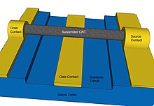
Nanoelectromechanical systems (NEMS) are a class of devices integrating electrical and mechanical functionality on the nanoscale. NEMS form the next logical miniaturization step from so-called microelectromechanical systems, or MEMS devices. NEMS typically integrate transistor-like nanoelectronics with mechanical actuators, pumps, or motors, and may thereby form physical, biological, and chemical sensors. The name derives from typical device dimensions in the nanometer range, leading to low mass, high mechanical resonance frequencies, potentially large quantum mechanical effects such as zero point motion, and a high surface-to-volume ratio useful for surface-based sensing mechanisms. Applications include accelerometers and sensors to detect chemical substances in the air.

<span class="mw-page-title-main">Threshold voltage</span> Minimum source-to-gate voltage for a field effect transistor to be conducting from source to drain

The threshold voltage, commonly abbreviated as Vth or VGS(th), of a field-effect transistor (FET) is the minimum gate-to-source voltage (VGS) that is needed to create a conducting path between the source and drain terminals. It is an important scaling factor to maintain power efficiency.

<span class="mw-page-title-main">Organic field-effect transistor</span> Type of field-effect transistor

An organic field-effect transistor (OFET) is a field-effect transistor using an organic semiconductor in its channel. OFETs can be prepared either by vacuum evaporation of small molecules, by solution-casting of polymers or small molecules, or by mechanical transfer of a peeled single-crystalline organic layer onto a substrate. These devices have been developed to realize low-cost, large-area electronic products and biodegradable electronics. OFETs have been fabricated with various device geometries. The most commonly used device geometry is bottom gate with top drain and source electrodes, because this geometry is similar to the thin-film silicon transistor (TFT) using thermally grown SiO2 as gate dielectric. Organic polymers, such as poly(methyl-methacrylate) (PMMA), can also be used as dielectric. One of the benefits of OFETs, especially compared with inorganic TFTs, is their unprecedented physical flexibility, which leads to biocompatible applications, for instance in the future health care industry of personalized biomedicines and bioelectronics.

Phaedon Avouris is a Greek chemical physicist and materials scientist. He is an IBM Fellow and was formerly the group leader for Nanometer Scale Science and Technology at the Thomas J. Watson Research Center in Yorktown Heights, New York.

Hybrid solar cells combine advantages of both organic and inorganic semiconductors. Hybrid photovoltaics have organic materials that consist of conjugated polymers that absorb light as the donor and transport holes. Inorganic materials in hybrid cells are used as the acceptor and electron transporter in the structure. The hybrid photovoltaic devices have a potential for not only low-cost by roll-to-roll processing but also for scalable solar power conversion.

<span class="mw-page-title-main">Potential applications of carbon nanotubes</span>

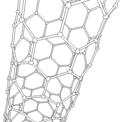
Carbon nanotubes (CNTs) are cylinders of one or more layers of graphene (lattice). Diameters of single-walled carbon nanotubes (SWNTs) and multi-walled carbon nanotubes (MWNTs) are typically 0.8 to 2 nm and 5 to 20 nm, respectively, although MWNT diameters can exceed 100 nm. CNT lengths range from less than 100 nm to 0.5 m.

In solid-state physics, a metal–semiconductor (M–S) junction is a type of electrical junction in which a metal comes in close contact with a semiconductor material. It is the oldest practical semiconductor device. M–S junctions can either be rectifying or non-rectifying. The rectifying metal–semiconductor junction forms a Schottky barrier, making a device known as a Schottky diode, while the non-rectifying junction is called an ohmic contact.

Organic photovoltaic devices (OPVs) are fabricated from thin films of organic semiconductors, such as polymers and small-molecule compounds, and are typically on the order of 100 nm thick. Because polymer based OPVs can be made using a coating process such as spin coating or inkjet printing, they are an attractive option for inexpensively covering large areas as well as flexible plastic surfaces. A promising low cost alternative to conventional solar cells made of crystalline silicon, there is a large amount of research being dedicated throughout industry and academia towards developing OPVs and increasing their power conversion efficiency.

A device generating linear or rotational motion using carbon nanotube(s) as the primary component, is termed a nanotube nanomotor. Nature already has some of the most efficient and powerful kinds of nanomotors. Some of these natural biological nanomotors have been re-engineered to serve desired purposes. However, such biological nanomotors are designed to work in specific environmental conditions. Laboratory-made nanotube nanomotors on the other hand are significantly more robust and can operate in diverse environments including varied frequency, temperature, mediums and chemical environments. The vast differences in the dominant forces and criteria between macroscale and micro/nanoscale offer new avenues to construct tailor-made nanomotors. The various beneficial properties of carbon nanotubes makes them the most attractive material to base such nanomotors on.

NanoIntegris is a nanotechnology company based in Boisbriand, Quebec specializing in the production of enriched, single-walled carbon nanotubes. In 2012, NanoIntegris was acquired by Raymor Industries, a large-scale producer of single-wall carbon nanotubes using the plasma torch process.

Single-walled carbon nanotubes in the fields of quantum mechanics and nanoelectronics, have the ability to conduct electricity. This conduction can be ballistic, diffusive, or based on scattering. When ballistic in nature conductance can be treated as if the electrons experience no scattering.

<span class="mw-page-title-main">Tunnel field-effect transistor</span>

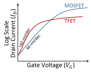
The tunnel field-effect transistor (TFET) is an experimental type of transistor. Even though its structure is very similar to a metal–oxide–semiconductor field-effect transistor (MOSFET), the fundamental switching mechanism differs, making this device a promising candidate for low power electronics. TFETs switch by modulating quantum tunneling through a barrier instead of modulating thermionic emission over a barrier as in traditional MOSFETs. Because of this, TFETs are not limited by the thermal Maxwell–Boltzmann tail of carriers, which limits MOSFET drain current subthreshold swing to about 60 mV/decade of current at room temperature.

Carbon nanotube computers are a class of experimental computing processors constructed from carbon nanotube field-effect transistors, instead of from conventional silicon-based field-effect transistors.

<span class="mw-page-title-main">Field-effect transistor</span> Type of transistor

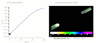
The field-effect transistor (FET) is a type of transistor that uses an electric field to control the flow of current in a semiconductor. It comes in two types: junction FET (JFET) and metal-oxide-semiconductor FET (MOSFET). FETs have three terminals: source, gate, and drain. FETs control the flow of current by the application of a voltage to the gate, which in turn alters the conductivity between the drain and source.

In nanotechnology, carbon nanotube interconnects refer to the proposed use of carbon nanotubes in the interconnects between the elements of an integrated circuit. Carbon nanotubes (CNTs) can be thought of as single atomic layer graphite sheets rolled up to form seamless cylinders. Depending on the direction on which they are rolled, CNTs can be semiconducting or metallic. Metallic carbon nanotubes have been identified as a possible interconnect material for the future technology generations and to replace copper interconnects. Electron transport can go over long nanotube lengths, 1 μm, enabling CNTs to carry very high currents (i.e. up to a current density of 109 A∙cm−2) with essentially no heating due to nearly one dimensional electronic structure. Despite the current saturation in CNTs at high fields, the mitigation of such effects is possible due to encapsulated nanowires.

In materials science, vertically aligned carbon nanotube arrays (VANTAs) are a unique microstructure consisting of carbon nanotubes oriented with their longitudinal axis perpendicular to a substrate surface. These VANTAs effectively preserve and often accentuate the unique anisotropic properties of individual carbon nanotubes and possess a morphology that may be precisely controlled. VANTAs are consequently widely useful in a range of current and potential device applications.

<span class="mw-page-title-main">Single-electron transistor</span>

A single-electron transistor (SET) is a sensitive electronic device based on the Coulomb blockade effect. In this device the electrons flow through a tunnel junction between source/drain to a quantum dot. Moreover, the electrical potential of the island can be tuned by a third electrode, known as the gate, which is capacitively coupled to the island. The conductive island is sandwiched between two tunnel junctions modeled by capacitors, and , and resistors, and , in parallel.

References

  1. 1 2 Dekker, Cees; Tans, Sander J.; Verschueren, Alwin R. M. (1998). "Room-temperature transistor based on a single carbon nanotube". Nature. 393 (6680): 49–52. Bibcode:1998Natur.393...49T. doi:10.1038/29954. S2CID   4403144.
  2. 1 2 Martel, R.; Schmidt, T.; Shea, H. R.; Hertel, T.; Avouris, Ph. (1998). "Single- and multi-wall carbon nanotube field-effect transistors" (PDF). Applied Physics Letters. 73 (17): 2447. Bibcode:1998ApPhL..73.2447M. doi:10.1063/1.122477.
  3. International Technology Roadmap for Semiconductors Archived August 25, 2011, at the Wayback Machine 2009 Edition
  4. Avouris, P; Chen, J (2006). "Nanotube electronics and optoelectronics". Materials Today. 9 (10): 46–54. doi: 10.1016/S1369-7021(06)71653-4 .
  5. H. Dai, A. Javey, E. Pop, D. Mann, Y. Lu, "Electrical Properties and Field-Effect Transistors of Carbon Nanotubes," Nano: Brief Reports and Reviews 1, 1 (2006).
  6. Collins, P.G.; Avouris, P. (2000). "Nanotubes for Electronics". Scientific American. 283 (6): 62–69. Bibcode:2000SciAm.283f..62C. doi:10.1038/scientificamerican1200-62. PMID   11103460.
  7. 1 2 3 Mintmire, J.W.; Dunlap, B.I.; White, C.T. (3 February 1992). "Are fullerene tubules metallic?". Phys. Rev. Lett. 68 (5): 631–634. Bibcode:1992PhRvL..68..631M. doi:10.1103/PhysRevLett.68.631. PMID   10045950.
  8. 1 2 3 4 5 Hamada, N.; Sawada, S.; Oshiyama, A. (9 March 1992). "New one-dimensional conductors: graphitic microtubules". Phys. Rev. Lett. 68 (10): 1579–1581. Bibcode:1992PhRvL..68.1579H. doi:10.1103/PhysRevLett.68.1579. PMID   10045167.
  9. 1 2 3 4 Dresselhaus, M.; Dresselhaus, G.; Saito, Riichiro (15 July 1992). "Carbon fibers based on C60 and their symmetry" (PDF). Physical Review B. 45 (11): 6234–6242. Bibcode:1992PhRvB..45.6234D. doi:10.1103/PhysRevB.45.6234. PMID   10000369. Archived from the original (PDF) on July 22, 2011.
  10. Iijima, Sumio (7 November 1991). "Helical microtubules of graphitic carbon". Nature. 354 (6348): 56–58. Bibcode:1991Natur.354...56I. doi:10.1038/354056a0. S2CID   4302490.
  11. 1 2 White, C. T.; Mintmire, J. W.; et al. (April 1993). "Chapter 6: Predicting Properties of Fullerenes and their Derivatives". In Billups, W . E.; Ciufolini, M. A. (eds.). Buckminsterfullerenes. VCH Publishers, Inc., New York, New York. p. 167. ISBN   1-56081-608-2.
  12. Ouyang, M; Huang, J. L.; Chung, C. L.; Lieber, C. M. (2001). "Energy Gaps in "metallic" single-walled carbon nanotubes". Science. 292 (5517): 702–705. Bibcode:2001Sci...292..702O. doi:10.1126/science.1058853. PMID   11326093. S2CID   19088925.
  13. White, C.T.; Robertson,D.H; Mintmire, J.W (1993). "Helical and rotational symmetries of nanoscale graphitic tubules". Phys. Rev. B. 68 (9): 5485–5488. Bibcode:1993PhRvB..47.5485W. doi:10.1103/PhysRevB.47.5485. PMID   10006726.
  14. Mintmire, J.W.; White, C.T. (1995). "Electronic and structural properties of carbon nanotubes". Carbon. 33 (7): 891–902. doi:10.1016/0008-6223(95)00018-9.
  15. Wildoer J.W.G.; Venema, L.C.; Rinzler, A.G.; Smalley, R.E.; Dekker, C. (1998). "Electronic structure of atomically resolved carbon nanotubes". Nature. 391 (6662): 58–62. Bibcode:1998Natur.391...59W. doi:10.1038/34139. S2CID   205003208.
  16. White, C.T.; Mintmire, J.W (2005). "Fundamental properties of single-wall carbon nanotubes". J. Phys. Chem. B. 109 (1): 52–65. doi:10.1021/jp047416. PMID   16850984.
  17. Heinze, S; Tersoff, J; Martel, R; Derycke, V; Appenzeller, J; Avouris, P (2002). "Carbon nanotubes as Schottky barrier transistors" (PDF). Physical Review Letters. 89 (10): 106801. arXiv: cond-mat/0207397 . Bibcode:2002PhRvL..89j6801H. doi:10.1103/PhysRevLett.89.106801. PMID   12225214. S2CID   119093126. Archived from the original (PDF) on December 3, 2008.
  18. 1 2 Wind, S. J.; Appenzeller, J.; Martel, R.; Derycke, V.; Avouris, Ph. (2002). "Vertical scaling of carbon nanotube field-effect transistors using top gate electrodes" (PDF). Applied Physics Letters. 80 (20): 3817. Bibcode:2002ApPhL..80.3817W. doi:10.1063/1.1480877. Archived from the original (PDF) on 2011-07-03.
  19. Lim, Seong Chu (November 2006). "A strategy for forming robust adhesion with the substrate in a carbon-nanotube field-emission array". Carbon. 44 (13): 2809. doi:10.1016/j.carbon.2006.03.030.
  20. Chen, Zhihong; Farmer, Damon; Xu, Sheng; Gordon, Roy; Avouris, Phaedon; Appenzeller, Joerg (2008). "Externally Assembled Gate-All-Around Carbon Nanotube Field-Effect Transistor". IEEE Electron Device Letters. 29 (2): 183–185. Bibcode:2008IEDL...29..183C. doi:10.1109/LED.2007.914069. S2CID   18509168.
  21. Farmer, DB; Gordon, RG (2006). "Atomic layer deposition on suspended single-walled carbon nanotubes via gas-phase noncovalent functionalization". Nano Letters. 6 (4): 699–703. Bibcode:2006NanoL...6..699F. doi:10.1021/nl052453d. PMID   16608267.
  22. 1 2 3 Cao, J; Wang, Q; Dai, H (2005). "Electron transport in very clean, as-grown suspended carbon nanotubes". Nature Materials. 4 (10): 745–9. arXiv: cond-mat/0509125 . Bibcode:2005NatMa...4..745C. doi:10.1038/nmat1478. PMID   16142240. S2CID   36444609.
  23. 1 2 Sangwan, V. K.; Ballarotto, V. W.; Fuhrer, M. S.; Williams, E. D. (2008). "Facile fabrication of suspended as-grown carbon nanotube devices". Applied Physics Letters. 93 (11): 113112. arXiv: 0909.3679 . Bibcode:2008ApPhL..93k3112S. doi:10.1063/1.2987457. S2CID   119260715.
  24. 1 2 Lin, Yu-Ming; Tsang, James C; Freitag, Marcus; Avouris, Phaedon (2007). "Impact of oxide substrate on electrical and optical properties of carbon nanotube devices" (PDF). Nanotechnology. 18 (29): 295202. Bibcode:2007Nanot..18C5202L. doi:10.1088/0957-4484/18/29/295202. S2CID   56534541.
  25. Javey, Ali; Guo, Jing; Wang, Qian; Lundstrom, Mark; Dai, Hongjie (2003). "Ballistic carbon nanotube field-effect transistors" (PDF). Nature. 424 (6949): 654–7. Bibcode:2003Natur.424..654J. doi:10.1038/nature01797. PMID   12904787. S2CID   1142790. Archived from the original (PDF) on July 24, 2008.
  26. Zhao, Y.; et al. (2014). "CNT Mobility". doi:10.4231/D3V698C9Z.{{cite journal}}: Cite journal requires |journal= (help)
  27. 1 2 Avouris, Phaedon; Chen, Zhihong; Perebeinos, Vasili (2007). "Carbon-based electronics". Nature Nanotechnology. 2 (10): 605–15. Bibcode:2007NatNa...2..605A. doi:10.1038/nnano.2007.300. PMID   18654384.
  28. P.Avouris et al, "Electronics and Optoelectronics with Carbon Nanotubes," Archived October 8, 2010, at the Wayback Machine American Institute of Physics, 18–21, June/July 2004. (pdf version Archived 2010-10-08 at the Wayback Machine )
  29. 1 2 S.Rasmita et al, "Simulation of Carbon Nanotube Field Effect Transistors," International Journal of Electronic Engineering Research, 117–125 Vol.1, No.2 (2009)
  30. 1 2 3 Kazmierski, Tom J.; Zhou, Dafeng; Al-Hashimi, Bashir M.; Ashburn, Peter (2010). "Numerically Efficient Modeling of CNT Transistors with Ballistic and Nonballistic Effects for Circuit Simulation" (PDF). IEEE Transactions on Nanotechnology. 9 (1): 99–107. Bibcode:2010ITNan...9...99K. doi:10.1109/TNANO.2009.2017019. S2CID   8846760.
  31. Ouyang, Yijian; Guo, Jing (2006). "Heat dissipation in carbon nanotube transistors". Applied Physics Letters. 89 (18): 183122. Bibcode:2006ApPhL..89r3122O. doi:10.1063/1.2382734.
  32. Jing Guo; Datta, S.; Lundstrom, M.; Brink, M.; McEuen, P.; Javey, A.; Hongjie Dai; Hyoungsub Kim; McIntyre, P. (2002). "Assessment of silicon MOS and carbon nanotube FET performance limits using a general theory of ballistic transistors" (PDF). Digest. International Electron Devices Meeting. p. 711. doi:10.1109/IEDM.2002.1175937. ISBN   0-7803-7462-2.
  33. Franklin, Aaron D.; Luisier, Mathieu; Han, Shu-Jen; Tulevski, George; Breslin, Chris M.; Gignac, Lynne; Lundstrom, Mark S.; Haensch, Wilfried (2012-02-08). "Sub-10 nm Carbon Nanotube Transistor". Nano Letters. 12 (2): 758–762. Bibcode:2012NanoL..12..758F. doi:10.1021/nl203701g. ISSN   1530-6984. PMID   22260387. S2CID   12194219.
  34. 1 2 Noyce, Steven G.; Doherty, James L.; Cheng, Zhihui; Han, Hui; Bowen, Shane; Franklin, Aaron D. (2019-02-05). "Electronic Stability of Carbon Nanotube Transistors Under Long-Term Bias Stress". Nano Letters. 19 (3). American Chemical Society (ACS): 1460–1466. Bibcode:2019NanoL..19.1460N. doi:10.1021/acs.nanolett.8b03986. ISSN   1530-6984. PMID   30720283. S2CID   73450707.
  35. Pop, Eric; Dutta, Sumit; Estrada, David; Liao, Albert (2009). "Avalanche, joule breakdown and hysteresis in carbon nanotube transistors" (PDF). 2009 IEEE International Reliability Physics Symposium (IRPS 2009). p. 405. doi:10.1109/IRPS.2009.5173287. ISBN   978-1-4244-2888-5.
  36. C.Changxin and Z.Yafei, "Nanowelded Carbon Nanotubes: From Field-Effect Transistor to Solar Microcells" Nano Science and Technology series (2009), pp. 63 ff ISBN   3-642-01498-4
  37. Chang-Jian, Shiang-Kuo; Ho, Jeng-Rong; John Cheng, J.-W. (2010). "Characterization of developing source/drain current of carbon nanotube field-effect transistors with n-doping by polyethylene imine". Microelectronic Engineering. 87 (10): 1973–1977. doi:10.1016/j.mee.2009.12.019.