Hall effect

Last updated
In diagram A, the flat conductor possesses a negative charge on the top (symbolized by the blue color) and a positive charge on the bottom (red color). In B and C, the direction of the electrical and the magnetic fields are changed respectively which switches the polarity of the charges around. In D, both fields change direction simultaneously which results in the same polarity as in diagram A.
electrons
flat conductor, which serves as a hall element (hall effect sensor)
magnet
magnetic field
power source Hall effect.png
In diagram A, the flat conductor possesses a negative charge on the top (symbolized by the blue color) and a positive charge on the bottom (red color). In B and C, the direction of the electrical and the magnetic fields are changed respectively which switches the polarity of the charges around. In D, both fields change direction simultaneously which results in the same polarity as in diagram A.
  1. electrons
  2. flat conductor, which serves as a hall element (hall effect sensor)
  3. magnet
  4. magnetic field
  5. power source

The Hall effect is the production of a potential difference (the Hall voltage) across an electrical conductor that is transverse to an electric current in the conductor and to an applied magnetic field perpendicular to the current. It was discovered by Edwin Hall in 1879. [1] [2]

Contents

The Hall coefficient is defined as the ratio of the induced electric field to the product of the current density and the applied magnetic field. It is a characteristic of the material from which the conductor is made, since its value depends on the type, number, and properties of the charge carriers that constitute the current.

Discovery

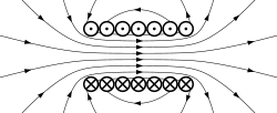
Wires carrying current in a magnetic field experience a mechanical force perpendicular to both the current and magnetic field. André-Marie Ampère in the 1820s observed this underlying mechanism that led to the discovery of the Hall effect. [3] However it was not until a solid mathematical basis for electromagnetism was systematized by James Clerk Maxwell's "On Physical Lines of Force" (published in 1861–1862) that details of the interaction between magnets and electric current could be understood.

Edwin Hall then explored the question of whether magnetic fields interacted with the conductors or the electric current, and reasoned that if the force was specifically acting on the current, it should crowd current to one side of the wire, producing a small measurable voltage. [3] In 1879, he discovered this Hall effect while he was working on his doctoral degree at Johns Hopkins University in Baltimore, Maryland. [4] Eighteen years before the electron was discovered, his measurements of the tiny effect produced in the apparatus he used were an experimental tour de force, published under the name "On a New Action of the Magnet on Electric Currents". [5] [6] [7]

Hall effect within voids

The term ordinary Hall effect can be used to distinguish the effect described in the introduction from a related effect which occurs across a void or hole in a semiconductor or metal plate when current is injected via contacts that lie on the boundary or edge of the void. The charge then flows outside the void, within the metal or semiconductor material. The effect becomes observable, in a perpendicular applied magnetic field, as a Hall voltage appearing on either side of a line connecting the current-contacts. It exhibits apparent sign reversal in comparison to the "ordinary" effect occurring in the simply connected specimen. It depends only on the current injected from within the void. [8]

Hall effect superposition

Superposition of these two forms of the effect, the ordinary and void effects, can also be realized. First imagine the "ordinary" configuration, a simply connected (void-less) thin rectangular homogeneous element with current-contacts on the (external) boundary. This develops a Hall voltage, in a perpendicular magnetic field. Next, imagine placing a rectangular void within this ordinary configuration, with current-contacts, as mentioned above, on the interior boundary of the void. (For simplicity, imagine the contacts on the boundary of the void lined up with the ordinary-configuration contacts on the exterior boundary.) In such a combined configuration, the two Hall effects may be realized and observed simultaneously in the same doubly connected device: A Hall effect on the external boundary that is proportional to the current injected only via the outer boundary, and an apparently sign-reversed Hall effect on the interior boundary that is proportional to the current injected only via the interior boundary. The superposition of multiple Hall effects may be realized by placing multiple voids within the Hall element, with current and voltage contacts on the boundary of each void. [8] [9]

Further "Hall effects" may have additional physical mechanisms but are built on these basics.

Theory

The Hall effect is due to the nature of the current in a conductor. Current consists of the movement of many small charge carriers, typically electrons, holes, ions (see Electromigration) or all three. When a magnetic field is present, these charges experience a force, called the Lorentz force. [10] When such a magnetic field is absent, the charges follow approximately straight paths between collisions with impurities, phonons, etc. However, when a magnetic field with a perpendicular component is applied, their paths between collisions are curved; thus, moving charges accumulate on one face of the material. This leaves equal and opposite charges exposed on the other face, where there is a scarcity of mobile charges. The result is an asymmetric distribution of charge density across the Hall element, arising from a force that is perpendicular to both the straight path and the applied magnetic field. The separation of charge establishes an electric field that opposes the migration of further charge, so a steady electric potential is established for as long as the charge is flowing. [11]

In classical electromagnetism electrons move in the opposite direction of the current I (by convention "current" describes a theoretical "hole flow"). In some metals and semiconductors it appears "holes" are actually flowing because the direction of the voltage is opposite to the derivation below.

Hall effect measurement setup for electrons. Initially, the electrons follow the curved arrow, due to the magnetic force. At some distance from the current-introducing contacts, electrons pile up on the left side and deplete from the right side, which creates an electric field xy in the direction of the assigned VH. VH is negative for some semiconductors where "holes" appear to flow. In steady-state, xy will be strong enough to exactly cancel out the magnetic force, thus the electrons follow the straight arrow (dashed). Hall Effect Measurement Setup for Electrons.png
Hall effect measurement setup for electrons. Initially, the electrons follow the curved arrow, due to the magnetic force. At some distance from the current-introducing contacts, electrons pile up on the left side and deplete from the right side, which creates an electric field ξy in the direction of the assigned VH. VH is negative for some semiconductors where "holes" appear to flow. In steady-state, ξy will be strong enough to exactly cancel out the magnetic force, thus the electrons follow the straight arrow (dashed).
The animation shows the action of a magnetic field on a beam of electric charges in vacuum, or in other terms, exclusively the action of the Lorentz force. This animation is an illustration of a typical error performed in the framework of the interpretation of the Hall effect. Indeed, at stationary regime and inside a Hall-bar, the electric current is longitudinal whatever the magnetic field and there is no transverse current (in contrast to the case of the corbino disc). Only the electric field is modified by a transverse component . [12]

For a simple metal where there is only one type of charge carrier (electrons), the Hall voltage VH can be derived by using the Lorentz force and seeing that, in the steady-state condition, charges are not moving in the y-axis direction. Thus, the magnetic force on each electron in the y-axis direction is cancelled by a y-axis electrical force due to the buildup of charges. The vx term is the drift velocity of the current which is assumed at this point to be holes by convention. The vxBz term is negative in the y-axis direction by the right hand rule.

In steady state, F = 0, so 0 = EyvxBz, where Ey is assigned in the direction of the y-axis, (and not with the arrow of the induced electric field ξy as in the image (pointing in the y direction), which tells you where the field caused by the electrons is pointing).

In wires, electrons instead of holes are flowing, so vx → −vx and q → −q. Also Ey = −VH/w. Substituting these changes gives

The conventional "hole" current is in the negative direction of the electron current and the negative of the electrical charge which gives Ix = ntw(−vx)(−e) where n is charge carrier density, tw is the cross-sectional area, and e is the charge of each electron. Solving for and plugging into the above gives the Hall voltage:

If the charge build up had been positive (as it appears in some metals and semiconductors), then the VH assigned in the image would have been negative (positive charge would have built up on the left side).

The Hall coefficient is defined as

or

where j is the current density of the carrier electrons, and Ey is the induced electric field. In SI units, this becomes

(The units of RH are usually expressed as m3/C, or Ω·cm/G, or other variants.) As a result, the Hall effect is very useful as a means to measure either the carrier density or the magnetic field.

One very important feature of the Hall effect is that it differentiates between positive charges moving in one direction and negative charges moving in the opposite. In the diagram above, the Hall effect with a negative charge carrier (the electron) is presented. But consider the same magnetic field and current are applied but the current is carried inside the Hall effect device by a positive particle. The particle would of course have to be moving in the opposite direction of the electron in order for the current to be the same—down in the diagram, not up like the electron is. And thus, mnemonically speaking, your thumb in the Lorentz force law, representing (conventional) current, would be pointing the same direction as before, because current is the same—an electron moving up is the same current as a positive charge moving down. And with the fingers (magnetic field) also being the same, interestingly the charge carrier gets deflected to the left in the diagram regardless of whether it is positive or negative. But if positive carriers are deflected to the left, they would build a relatively positive voltage on the left whereas if negative carriers (namely electrons) are, they build up a negative voltage on the left as shown in the diagram. Thus for the same current and magnetic field, the electric polarity of the Hall voltage is dependent on the internal nature of the conductor and is useful to elucidate its inner workings.

This property of the Hall effect offered the first real proof that electric currents in most metals are carried by moving electrons, not by protons. It also showed that in some substances (especially p-type semiconductors), it is contrarily more appropriate to think of the current as positive "holes" moving rather than negative electrons. A common source of confusion with the Hall effect in such materials is that holes moving one way are really electrons moving the opposite way, so one expects the Hall voltage polarity to be the same as if electrons were the charge carriers as in most metals and n-type semiconductors. Yet we observe the opposite polarity of Hall voltage, indicating positive charge carriers. However, of course there are no actual positrons or other positive elementary particles carrying the charge in p-type semiconductors, hence the name "holes". In the same way as the oversimplistic picture of light in glass as photons being absorbed and re-emitted to explain refraction breaks down upon closer scrutiny, this apparent contradiction too can only be resolved by the modern quantum mechanical theory of quasiparticles wherein the collective quantized motion of multiple particles can, in a real physical sense, be considered to be a particle in its own right (albeit not an elementary one). [13]

Unrelatedly, inhomogeneity in the conductive sample can result in a spurious sign of the Hall effect, even in ideal van der Pauw configuration of electrodes. For example, a Hall effect consistent with positive carriers was observed in evidently n-type semiconductors. [14] Another source of artefact, in uniform materials, occurs when the sample's aspect ratio is not long enough: the full Hall voltage only develops far away from the current-introducing contacts, since at the contacts the transverse voltage is shorted out to zero.

Hall effect in semiconductors

When a current-carrying semiconductor is kept in a magnetic field, the charge carriers of the semiconductor experience a force in a direction perpendicular to both the magnetic field and the current. At equilibrium, a voltage appears at the semiconductor edges.

The simple formula for the Hall coefficient given above is usually a good explanation when conduction is dominated by a single charge carrier. However, in semiconductors and many metals the theory is more complex, because in these materials conduction can involve significant, simultaneous contributions from both electrons and holes, which may be present in different concentrations and have different mobilities. For moderate magnetic fields the Hall coefficient is [15] [16]

or equivalently

with

Here n is the electron concentration, p the hole concentration, μe the electron mobility, μh the hole mobility and e the elementary charge.

For large applied fields the simpler expression analogous to that for a single carrier type holds.

Relationship with star formation

Although it is well known that magnetic fields play an important role in star formation, research models [17] [18] [19] indicate that Hall diffusion critically influences the dynamics of gravitational collapse that forms protostars.

Quantum Hall effect

For a two-dimensional electron system which can be produced in a MOSFET, in the presence of large magnetic field strength and low temperature, one can observe the quantum Hall effect, in which the Hall conductance σ undergoes quantum Hall transitions to take on the quantized values.

Spin Hall effect

The spin Hall effect consists in the spin accumulation on the lateral boundaries of a current-carrying sample. No magnetic field is needed. It was predicted by Mikhail Dyakonov and V. I. Perel in 1971 and observed experimentally more than 30 years later, both in semiconductors and in metals, at cryogenic as well as at room temperatures.

The quantity describing the strength of the Spin Hall effect is known as Spin Hall angle, and it is defined as:

Where is the spin current generated by the applied current density . [20]

Quantum spin Hall effect

For mercury telluride two dimensional quantum wells with strong spin-orbit coupling, in zero magnetic field, at low temperature, the quantum spin Hall effect has been observed in 2007. [21]

Anomalous Hall effect

In ferromagnetic materials (and paramagnetic materials in a magnetic field), the Hall resistivity includes an additional contribution, known as the anomalous Hall effect (or the extraordinary Hall effect), which depends directly on the magnetization of the material, and is often much larger than the ordinary Hall effect. (Note that this effect is not due to the contribution of the magnetization to the total magnetic field.) For example, in nickel, the anomalous Hall coefficient is about 100 times larger than the ordinary Hall coefficient near the Curie temperature, but the two are similar at very low temperatures. [22] Although a well-recognized phenomenon, there is still debate about its origins in the various materials. The anomalous Hall effect can be either an extrinsic (disorder-related) effect due to spin-dependent scattering of the charge carriers, or an intrinsic effect which can be described in terms of the Berry phase effect in the crystal momentum space (k-space). [23]

Hall effect in ionized gases

The Hall effect in an ionized gas (plasma) is significantly different from the Hall effect in solids (where the Hall parameter is always much less than unity). In a plasma, the Hall parameter can take any value. The Hall parameter, β, in a plasma is the ratio between the electron gyrofrequency, Ωe, and the electron-heavy particle collision frequency, ν:

where

The Hall parameter value increases with the magnetic field strength.

Physically, the trajectories of electrons are curved by the Lorentz force. Nevertheless, when the Hall parameter is low, their motion between two encounters with heavy particles (neutral or ion) is almost linear. But if the Hall parameter is high, the electron movements are highly curved. The current density vector, J, is no longer collinear with the electric field vector, E. The two vectors J and E make the Hall angle, θ, which also gives the Hall parameter:

Other Hall effects

The Hall Effects family has expanded to encompass other quasi-particles in semiconductor nanostructures. Specifically, a set of Hall Effects has emerged based on excitons [24] [25] and exciton-polaritons [26] n 2D materials and quantum wells.

Applications

Hall sensors amplify and use the Hall effect for a variety of sensing applications.

Corbino effect

Corbino disc - dashed curves represent logarithmic spiral paths of deflected electrons Corbino disc by Zureks.svg
Corbino disc – dashed curves represent logarithmic spiral paths of deflected electrons

The Corbino effect, named after its discoverer Orso Mario Corbino, is a phenomenon involving the Hall effect, but a disc-shaped metal sample is used in place of a rectangular one. Because of its shape the Corbino disc allows the observation of Hall effect–based magnetoresistance without the associated Hall voltage.

A radial current through a circular disc, subjected to a magnetic field perpendicular to the plane of the disc, produces a "circular" current through the disc. [27]

The absence of the free transverse boundaries renders the interpretation of the Corbino effect simpler than that of the Hall effect.

See also

Related Research Articles

<span class="mw-page-title-main">Ohm's law</span> Law of electrical current and voltage

Ohm's law states that the electric current through a conductor between two points is directly proportional to the voltage across the two points. Introducing the constant of proportionality, the resistance, one arrives at the three mathematical equations used to describe this relationship:

The quantum Hall effect is a quantized version of the Hall effect which is observed in two-dimensional electron systems subjected to low temperatures and strong magnetic fields, in which the Hall resistance Rxy exhibits steps that take on the quantized values

<span class="mw-page-title-main">Electromotive force</span> Electrical action produced by a non-electrical source

In electromagnetism and electronics, electromotive force is an energy transfer to an electric circuit per unit of electric charge, measured in volts. Devices called electrical transducers provide an emf by converting other forms of energy into electrical energy. Other electrical equipment also produce an emf, such as batteries, which convert chemical energy, and generators, which convert mechanical energy. This energy conversion is achieved by physical forces applying physical work on electric charges. However, electromotive force itself is not a physical force, and ISO/IEC standards have deprecated the term in favor of source voltage or source tension instead.

<span class="mw-page-title-main">Capacitance</span> Ability of a body to store an electrical charge

Capacitance is the capability of a material object or device to store electric charge. It is measured by the charge in response to a difference in electric potential, expressed as the ratio of those quantities. Commonly recognized are two closely related notions of capacitance: self capacitance and mutual capacitance. An object that can be electrically charged exhibits self capacitance, for which the electric potential is measured between the object and ground. Mutual capacitance is measured between two components, and is particularly important in the operation of the capacitor, an elementary linear electronic component designed to add capacitance to an electric circuit.

In solid state physics, a particle's effective mass is the mass that it seems to have when responding to forces, or the mass that it seems to have when interacting with other identical particles in a thermal distribution. One of the results from the band theory of solids is that the movement of particles in a periodic potential, over long distances larger than the lattice spacing, can be very different from their motion in a vacuum. The effective mass is a quantity that is used to simplify band structures by modeling the behavior of a free particle with that mass. For some purposes and some materials, the effective mass can be considered to be a simple constant of a material. In general, however, the value of effective mass depends on the purpose for which it is used, and can vary depending on a number of factors.

In physics, screening is the damping of electric fields caused by the presence of mobile charge carriers. It is an important part of the behavior of charge-carrying fluids, such as ionized gases, electrolytes, and charge carriers in electronic conductors . In a fluid, with a given permittivity ε, composed of electrically charged constituent particles, each pair of particles interact through the Coulomb force as

<span class="mw-page-title-main">Ampère's circuital law</span> Concept in classical electromagnetism

In classical electromagnetism, Ampère's circuital law relates the circulation of a magnetic field around a closed loop to the electric current passing through the loop.

Space charge is an interpretation of a collection of electric charges in which excess electric charge is treated as a continuum of charge distributed over a region of space rather than distinct point-like charges. This model typically applies when charge carriers have been emitted from some region of a solid—the cloud of emitted carriers can form a space charge region if they are sufficiently spread out, or the charged atoms or molecules left behind in the solid can form a space charge region.

The van der Pauw Method is a technique commonly used to measure the resistivity and the Hall coefficient of a sample. Its power lies in its ability to accurately measure the properties of a sample of any arbitrary shape, as long as the sample is approximately two-dimensional, solid, and the electrodes are placed on its perimeter. The van der Pauw method employs a four-point probe placed around the perimeter of the sample, in contrast to the linear four point probe: this allows the van der Pauw method to provide an average resistivity of the sample, whereas a linear array provides the resistivity in the sensing direction. This difference becomes important for anisotropic materials, which can be properly measured using the Montgomery Method, an extension of the van der Pauw Method.

<span class="mw-page-title-main">Magnetic moment</span> Magnetic strength and orientation of an object that produces a magnetic field

In electromagnetism, the magnetic moment or magnetic dipole moment is the combination of strength and orientation of a magnet or other object or system that exerts a magnetic field. The magnetic dipole moment of an object determines the magnitude of torque the object experiences in a given magnetic field. When the same magnetic field is applied, objects with larger magnetic moments experience larger torques. The strength of this torque depends not only on the magnitude of the magnetic moment but also on its orientation relative to the direction of the magnetic field. Its direction points from the south pole to north pole of the magnet.

p–n junction Semiconductor–semiconductor junction

A p–n junction is a combination of two types of semiconductor materials, p-type and n-type, in a single crystal. The "n" (negative) side contains freely-moving electrons, while the "p" (positive) side contains freely-moving electron holes. Connecting the two materials causes creation of a depletion region near the boundary, as the free electrons fill the available holes, which in turn allows electric current to pass through the junction only in one direction.

In solid-state physics, the electron mobility characterises how quickly an electron can move through a metal or semiconductor when pushed or pulled by an electric field. There is an analogous quantity for holes, called hole mobility. The term carrier mobility refers in general to both electron and hole mobility.

<span class="mw-page-title-main">Seebeck coefficient</span> Measure of voltage induced by change of temperature

The Seebeck coefficient of a material is a measure of the magnitude of an induced thermoelectric voltage in response to a temperature difference across that material, as induced by the Seebeck effect. The SI unit of the Seebeck coefficient is volts per kelvin (V/K), although it is more often given in microvolts per kelvin (μV/K).

<span class="mw-page-title-main">Tunnel magnetoresistance</span> Magnetic effect in insulators between ferromagnets

Tunnel magnetoresistance (TMR) is a magnetoresistive effect that occurs in a magnetic tunnel junction (MTJ), which is a component consisting of two ferromagnets separated by a thin insulator. If the insulating layer is thin enough, electrons can tunnel from one ferromagnet into the other. Since this process is forbidden in classical physics, the tunnel magnetoresistance is a strictly quantum mechanical phenomenon, and lies in the study of spintronics.

In solid-state physics, the free electron model is a quantum mechanical model for the behaviour of charge carriers in a metallic solid. It was developed in 1927, principally by Arnold Sommerfeld, who combined the classical Drude model with quantum mechanical Fermi–Dirac statistics and hence it is also known as the Drude–Sommerfeld model.

In semiconductor physics, the depletion region, also called depletion layer, depletion zone, junction region, space charge region, or space charge layer, is an insulating region within a conductive, doped semiconductor material where the mobile charge carriers have diffused away, or forced away by an electric field. The only elements left in the depletion region are ionized donor or acceptor impurities. This region of uncovered positive and negative ions is called the depletion region due to the depletion of carriers in this region, leaving none to carry a current. Understanding the depletion region is key to explaining modern semiconductor electronics: diodes, bipolar junction transistors, field-effect transistors, and variable capacitance diodes all rely on depletion region phenomena.

In solid-state physics, the thermal Hall effect, also known as the Righi–Leduc effect, named after independent co-discoverers Augusto Righi and Sylvestre Anatole Leduc, is the thermal analog of the Hall effect. Given a thermal gradient across a solid, this effect describes the appearance of an orthogonal temperature gradient when a magnetic field is applied.

Diffusion current is a current in a semiconductor caused by the diffusion of charge carriers. This is the current which is due to the transport of charges occurring because of non-uniform concentration of charged particles in a semiconductor. The drift current, by contrast, is due to the motion of charge carriers due to the force exerted on them by an electric field. Diffusion current can be in the same or opposite direction of a drift current. The diffusion current and drift current together are described by the drift–diffusion equation.

The Rashba effect, also called Bychkov–Rashba effect, is a momentum-dependent splitting of spin bands in bulk crystals and low-dimensional condensed matter systems similar to the splitting of particles and anti-particles in the Dirac Hamiltonian. The splitting is a combined effect of spin–orbit interaction and asymmetry of the crystal potential, in particular in the direction perpendicular to the two-dimensional plane. This effect is named in honour of Emmanuel Rashba, who discovered it with Valentin I. Sheka in 1959 for three-dimensional systems and afterward with Yurii A. Bychkov in 1984 for two-dimensional systems.

Electric dipole spin resonance (EDSR) is a method to control the magnetic moments inside a material using quantum mechanical effects like the spin–orbit interaction. Mainly, EDSR allows to flip the orientation of the magnetic moments through the use of electromagnetic radiation at resonant frequencies. EDSR was first proposed by Emmanuel Rashba.

References

  1. Edwin Hall (1879). "On a New Action of the Magnet on Electric Currents". American Journal of Mathematics. 2 (3): 287–92. doi:10.2307/2369245. JSTOR   2369245. S2CID   107500183. Archived from the original on 2011-07-27. Retrieved 2008-02-28.
  2. "Hall effect | Definition & Facts". Encyclopedia Britannica. Retrieved 2020-02-13.
  3. 1 2 Ramsden, Edward (2011-04-01). Hall-Effect Sensors: Theory and Application. Elsevier. p. 2. ISBN   978-0-08-052374-3.
  4. Bridgeman, P. W. (1939). Biographical Memoir of Edwin Herbert Hall. National Academy of Sciences.
  5. Hall, E. H. (1879). "On a New Action of the Magnet on Electric Currents". American Journal of Mathematics. 2 (3). JSTOR: 287–292. doi: 10.2307/2369245 . ISSN   0002-9327. JSTOR   2369245.
  6. "Hall Effect History". Archived from the original on 29 May 2015. Retrieved 2015-07-26.
  7. Ramsden, Edward (2006). Hall-Effect Sensors. Elsevier Inc. pp. xi. ISBN   978-0-7506-7934-3.
  8. 1 2 Mani, R. G.; von Klitzing, K. (1994-03-07). "Hall effect under null current conditions". Applied Physics Letters. 64 (10): 1262–1264. Bibcode:1994ApPhL..64.1262M. doi:10.1063/1.110859. ISSN   0003-6951.
  9. DEPatent 4308375
  10. "The Hall Effect". NIST. Archived from the original on 2008-03-07. Retrieved 2008-02-28.
  11. "Hall Effect Sensor". Electronic Tutorials.
  12. Creff, M.; Faisant, F.; Rubì, J. M.; Wegrowe, J.-E. (2020-08-07). "Surface currents in Hall devices". Journal of Applied Physics. 128 (5): 054501. arXiv: 1908.06282 . Bibcode:2020JAP...128e4501C. doi:10.1063/5.0013182. hdl:2445/176859. ISSN   0021-8979. S2CID   201070551.
  13. N.W. Ashcroft and N.D. Mermin "Solid State Physics" ISBN   978-0-03-083993-1
  14. Ohgaki, Takeshi; Ohashi, Naoki; Sugimura, Shigeaki; Ryoken, Haruki; Sakaguchi, Isao; Adachi, Yutaka; Haneda, Hajime (2008). "Positive Hall coefficients obtained from contact misplacement on evident n-type ZnO films and crystals". Journal of Materials Research. 23 (9): 2293. Bibcode:2008JMatR..23.2293O. doi:10.1557/JMR.2008.0300. S2CID   137944281.
  15. Kasap, Safa. "Hall Effect in Semiconductors" (PDF). Archived from the original (PDF) on 2008-08-21.
  16. "Hall Effect". hyperphysics.phy-astr.gsu.edu. Retrieved 2020-02-13.
  17. Mark Wardle (2004). "Star Formation and the Hall Effect". Astrophysics and Space Science. 292 (1): 317–323. arXiv: astro-ph/0307086 . Bibcode:2004Ap&SS.292..317W. CiteSeerX   10.1.1.746.8082 . doi:10.1023/B:ASTR.0000045033.80068.1f. S2CID   119027877.
  18. Braiding, C. R.; Wardle, M. (2012). "The Hall effect in star formation". Monthly Notices of the Royal Astronomical Society. 422 (1): 261. arXiv: 1109.1370 . Bibcode:2012MNRAS.422..261B. doi:10.1111/j.1365-2966.2012.20601.x. S2CID   119280669.
  19. Braiding, C. R.; Wardle, M. (2012). "The Hall effect in accretion flows". Monthly Notices of the Royal Astronomical Society. 427 (4): 3188. arXiv: 1208.5887 . Bibcode:2012MNRAS.427.3188B. doi:10.1111/j.1365-2966.2012.22001.x. S2CID   118410321.
  20. Deng, Yongcheng; Yang, Meiyin; Ji, Yang; Wang, Kaiyou (2020-02-15). "Estimating spin Hall angle in heavy metal/ferromagnet heterostructures". Journal of Magnetism and Magnetic Materials. 496: 165920. Bibcode:2020JMMM..49665920D. doi:10.1016/j.jmmm.2019.165920. ISSN   0304-8853. S2CID   209989182.
  21. König, Markus; Wiedmann, Steffen; Brüne, Christoph; Roth, Andreas; Buhmann, Hartmut; Molenkamp, Laurens W.; Qi, Xiao-Liang; Zhang, Shou-Cheng (2007-11-02). "Quantum Spin Hall Insulator State in HgTe Quantum Wells". Science. 318 (5851): 766–770. arXiv: 0710.0582 . Bibcode:2007Sci...318..766K. doi:10.1126/science.1148047. ISSN   0036-8075. PMID   17885096. S2CID   8836690.
  22. Robert Karplus and J. M. Luttinger (1954). "Hall Effect in Ferromagnetics". Phys. Rev. 95 (5): 1154–1160. Bibcode:1954PhRv...95.1154K. doi:10.1103/PhysRev.95.1154.
  23. N. A. Sinitsyn (2008). "Semiclassical Theories of the Anomalous Hall Effect". Journal of Physics: Condensed Matter. 20 (2): 023201. arXiv: 0712.0183 . Bibcode:2008JPCM...20b3201S. doi:10.1088/0953-8984/20/02/023201. S2CID   1257769.
  24. Onga, Masaru; Zhang, Yijin; Ideue, Toshiya; Iwasa, Yoshihiro (December 2017). "Exciton Hall effect in monolayer MoS2". Nature Materials. 16 (12): 1193–1197. doi:10.1038/nmat4996. ISSN   1476-4660.
  25. Kozin, V. K.; Shabashov, V. A.; Kavokin, A. V.; Shelykh, I. A. (21 January 2021). "Anomalous Exciton Hall Effect". Physical Review Letters. 126 (3): 036801. arXiv: 2006.08717 . doi:10.1103/PhysRevLett.126.036801.
  26. Kavokin, Alexey; Malpuech, Guillaume; Glazov, Mikhail (19 September 2005). "Optical Spin Hall Effect". Physical Review Letters. 95 (13): 136601. doi:10.1103/PhysRevLett.95.136601.
  27. Adams, E. P. (1915). The Hall and Corbino effects. Vol. 54. pp. 47–51. Bibcode:1916PhDT.........2C. ISBN   978-1-4223-7256-2 . Retrieved 2009-01-24.{{cite book}}: |journal= ignored (help)

Sources

Further reading