Transition metal dichalcogenide monolayers

Last updated
(a) Structure of a hexagonal TMD monolayer. M atoms are in black and X atoms are in yellow. (b) A hexagonal TMD monolayer seen from above. Monolayer TMDC structure.jpg
(a) Structure of a hexagonal TMD monolayer. M atoms are in black and X atoms are in yellow. (b) A hexagonal TMD monolayer seen from above.

Transition-metal dichalcogenide (TMD or TMDC) monolayers are atomically thin semiconductors of the type MX2, with M a transition-metal atom (Mo, W, etc.) and X a chalcogen atom (S, Se, or Te). One layer of M atoms is sandwiched between two layers of X atoms. They are part of the large family of so-called 2D materials, named so to emphasize their extraordinary thinness. For example, a MoS2 monolayer is only 6.5 Å thick. The key feature of these materials is the interaction of large atoms in the 2D structure as compared with first-row transition-metal dichalcogenides, e.g., WTe2 exhibits anomalous giant magnetoresistance and superconductivity. [1]

Contents

The discovery of graphene shows how new physical properties emerge when a bulk crystal of macroscopic dimensions is thinned down to one atomic layer. Like graphite, TMD bulk crystals are formed of monolayers bound to each other by van-der-Waals attraction. TMD monolayers have properties that are distinctly different from those of the semimetal graphene:

The work on TMD monolayers is an emerging research and development field since the discovery of the direct bandgap [2] and the potential applications in electronics [14] [3] and valley physics. [7] [8] [9] TMDs are often combined with other 2D materials like graphene and hexagonal boron nitride to make van der Waals heterostructures. These heterostructures need to be optimized to be possibly used as building blocks for many different devices such as transistors, solar cells, LEDs, photodetectors, fuel cells, photocatalytic and sensing devices. Some of these devices are already used in everyday life and can become smaller, cheaper and more efficient by using TMD monolayers. [15] [16]

Crystal structure

Crystal structure of TMDs Molybdenite-3D-balls.png
Crystal structure of TMDs

Transition-metal dichalcogenides (TMDs) are composed of three atomic planes and often two atomic species: a metal and two chalcogens. The honeycomb, hexagonal lattice has threefold symmetry and can permit mirror plane symmetry and/or inversion symmetry. [17] In the macroscopic bulk crystal, or more precisely, for an even number of monolayers, the crystal structure has an inversion center. In the case of a monolayer (or any odd number of layers), the crystal may or may not have an inversion center.

Broken inversion symmetry

Two important consequences of that are:

These properties indicate that TMD monolayers represent a promising platform to explore spin and valley physics with the corresponding possible applications.

Properties

Transport properties

Representative scheme of the section of a field effect transistor based on a monolayer of MoS2 Field Effect Transistor MoS2.jpg
Representative scheme of the section of a field effect transistor based on a monolayer of MoS2

At submicron scales, 3D materials no longer have the same behavior as their 2D form, which can be an advantage. For example, graphene has a very high carrier mobility, and accompanying lower losses through the Joule effect. But graphene has zero bandgap, which results in a disqualifyingly low on/off ratio in transistor applications. TMD monolayers might be an alternative: they are structurally stable, display a band gap and show electron mobilities comparable to those of silicon, so they can be used to fabricate transistors.

Although thin-layer TMDs have been found to have a lower electron mobility than bulk TMDs, most likely because their thinness makes them more susceptible to damage, it has been found that coating the TMDs with HfO2 or hexagonal boron nitride (hBN) increases their effective carrier mobility. [25]

Optical properties

Theoretical energies of the A and B excitons [26]
A (eV) A (nm) B (eV) B (nm)
MoS21.78 695 1.96 632
MoSe21.50 825 1.75 708
MoTe21.06 1170 1.36 912
WS21.84 673 2.28 544
WSe21.52 815 2.00 620

A semiconductor can absorb photons with energy larger than or equal to its bandgap. This means that light with a shorter wavelength is absorbed. Semiconductors are typically efficient emitters if the minimum of the conduction band energy is at the same position in k-space as the maximum of the valence band, i.e., the band gap is direct. The band gap of bulk TMD material down to a thickness of two monolayers is still indirect, so the emission efficiency is lower compared to monolayered materials. The emission efficiency is about 104 greater for TMD monolayer than for bulk material. [4] The band gaps of TMD monolayers are in the visible range (between 400 nm and 700 nm). The direct emission shows two excitonic transitions called A and B, separated by the spin–orbit coupling energy. The lowest energy and therefore most important in intensity is the A emission. [2] [27] Owing to their direct band gap, TMD monolayers are promising materials for optoelectronics applications.

Representative scheme of the section of an ultrasensitive photodetector based on a monolayer of MoS2 Fotodetector de MoS2.jpg
Representative scheme of the section of an ultrasensitive photodetector based on a monolayer of MoS2

Atomic layers of MoS2 have been used as a phototransistor and ultrasensitive detectors. Phototransistors are important devices: the first with a MoS2 monolayer active region shows a photoresponsivity of 7.5 mA W−1 which is similar to graphene devices that reach 6.1 mA W−1. Multilayer MoS2 show higher photoresponsivities, about 100 mA W−1, which is similar to silicon devices. Making a gold contact at the far edges of a monolayer allows an ultrasensitive detector to be fabricated. [5] Such a detector has a photoresponsivity reaching 880 A W−1, 106 greater than the first graphene photodetectors. This high degree of electrostatic control is due to the thin active region of the monolayer. Its simplicity and the fact that it has only one semiconductor region, whereas the current generation of photodetectors is typically a p–n junction, makes possible industrial applications such as high-sensitivity and flexible photodetectors. The only limitation for currently available devices is the slow photoresponse dynamics. [5] Utilizing WSe2 the photoresponse was improved to a bandwidth of over 230 MHz by device symmetry optimization [28]

Mechanical properties

Interest in the use of TMD monolayers such as MoS2, WS2, and WSe2 for the use in flexible electronics due to a change from an indirect band gap in 3D to a direct band gap in 2D emphasizes the importance of the mechanical properties of these materials. [29] Unlike in bulk samples it is much more difficult to uniformly deform 2D monolayers of material and as a result, taking mechanical measurements of 2D systems is more challenging. A method that was developed to overcome this challenge, called atomic force microscopy (AFM) nanoindentation, involves bending a 2D monolayer suspended over a holey substrate with an AFM cantilever and measuring the applied force and displacement. [30] Through this method, defect free mechanically exfoliated monolayer flakes of MoS2 were found to have a Young's modulus of 270 GPa with a maximum experienced strain of 10% before breaking. [31] In the same study, it was found that bilayer mechanically exfoliated MoS2 flakes have a lower Young's modulus of 200 GPa, which is attributed to interlayer sliding and defects in the monolayer. [31] With increasing flake thickness the bending rigidity of the flake plays a dominant role and it is found that the Young's modulus of multilayer, 5- 25 layers, mechanically exfoliated MoS2 flakes is 330 GPa. [32]

The mechanical properties of other TMDs such as WS2 and WSe2 have also been determined. The Young's modulus of multilayer, 5-14 layers, mechanically exfoliated WSe2 is found to be 167 GPa with a maximum strain of 7%. [33] For WS2, the Young's modulus of chemical vapor deposited monolayer flakes is 272 GPa. [34] From this same study the Young's modulus of CVD-grown monolayer flakes of MoS2 is found to be 264 GPa. [34] This is an interesting result as the Young's modulus of the exfoliated MoS2 flake is nearly the same as that of the CVD grown MoS2 flake. It is generally accepted that chemically vapor deposited TMDs will include more defects when compared with the mechanically exfoliated films that are obtained from bulk single crystals, which implies that defects (points defects, etc.) that are included in the flake do not drastically affect the strength of the flake itself.

Under the application of strain, a decrease in the direct and indirect band gap is measured that is approximately linear with strain. [35] Importantly, the indirect bandgap decreases faster with applied strain to the monolayer than the direct bandgap, resulting in a crossover from direct to indirect band gap at a strain level of around 1%. [36] As a result, the emission efficiency of monolayers is expected to decrease for highly strained samples. [37] This property allows mechanical tuning of the electronic structure and also the possibility of fabrication of devices on flexible substrates.

Fabrication of TMD monolayers

Exfoliation

Exfoliation is a top down approach. In the bulk form, TMDs are crystals made of layers, which are coupled by Van-der-Waals forces. These interactions are weaker than the chemical bonds between the Mo and S in MoS2, for example. So TMD monolayers can be produced by micromechanical cleavage, just as graphene.

The crystal of TMD is rubbed against the surface of another material (any solid surface). In practice, adhesive tape is placed on the TMD bulk material and subsequently removed. The adhesive tape, with tiny TMD flakes coming off the bulk material, is brought down onto a substrate. On removing the adhesive tape from the substrate, TMD monolayer and multilayer flakes are deposited. This technique produces small samples of monolayer material, typically about 5–10 micrometers in diameter. [38]

Large quantities of exfoliated material can also be produced using liquid-phase exfoliation by blending TMD materials with solvents and polymers. [39]

Chemical vapor deposition

Chemical vapor deposition (CVD) is another approach used to synthesize transition-metal dichalcogenides. [40] It has been used broadly to synthesize many different TMDs because it can be easily adapted for different TMD materials. Generally, CVD growth of TMDs is achieved by putting precursors to the material, typically a transition-metal oxide and pure chalcogen, into a furnace with the substrate on which the material will form. [41] The furnace is heated to high temperatures (anywhere from 650 to 1000 °C) with an inert gas, typically N2 or Ar, flowing through the tube. [41] Some materials require H2 gas as a catalyst for formation, so it may be flowed through the furnace in smaller quantities than the inert gas. [42]

Outside of traditional CVD, metal organic chemical vapor deposition (MOCVD) has been used to synthesize TMDs. Unlike traditional CVD described above, MOCVD uses gaseous precursors, as opposed to solid precursors and MOCVD is usually carried out at lower temperatures, anywhere from 300 to 900 °C. [43] MOCVD has been shown to provide more consistent wafer-scale growth than traditional CVD.

CVD is often used over mechanical exfoliation despite its added complexity because it can produce monolayers ranging anywhere from 5 to 100 microns in size as opposed to the surface areas of roughly 5-10 microns produced using the mechanical exfoliation method. [44] Not only do TMD monolayers produced by CVD have a larger surface area than those flakes produced by mechanical exfoliation, they are often more uniform. Monolayer TMD flakes with very little or no multilayer areas can be produced by chemical vapor deposition, in contrast to samples produced by mechanical exfoliation, which often have many multilayered areas. [38] [41] Geometrically confined-growth techniques are also recently applied to realize wafer-scale single-domain TMD monolayer arrays and their heterostructures. [45]

Molecular-beam epitaxy

Molecular-beam epitaxy (MBE) is an established technique for growing semiconductor devices with atomic monolayer thickness control. MBE has been used to grow different TMDs, such as MoSe2, WSe2, and early transition metals, including titanium, vanadium, and chromium, tellurides, [46] [47] [48] resulting in extremely clean samples with a thickness of only 0.5 monolayer. [46] [48]

The growth takes place in ultra-high vacuum (UHV). Precursors for the target materials are placed into evaporation cells, usually as powder (for example selenium), or as a rod (for example molybdenum). [46] Some elements, such as selenium and tellurium, both of which are chalcogens, can be used in pure solid form as precursors. Some elements, however, can only be used when extracted from solid compounds, such as sulfur from FeS2. The compound materials are broken down by heating up the material at UHV pressures. [49] The evaporation cells are either Knudsen cells or electron beam evaporation based, depending on the materials; electron beam evaporation works with rods and can be used to reach high temperatures without overheating heating filaments, while Knudsen cells are suitable for powders and materials with a lower evaporation point. The evaporated materials are then directed towards the substrate; some common ones are MoS2, HOPG, mica, or a sapphire substrate, such as Al2O3. [46] [47] [48] [50] A specific substrate is chosen to fit the targeted growth the best. The substrate is kept heated during the process to enhance the growth, with the temperatures ranging from 300 °C to 700 °C. The temperature of the substrate is one key factor of the growth, and altering it can be used to grow different phases, such as 1T and 2H, of the same material. [46]

MBE holds some advantages in regards to both manual exfoliation and CVD. Use of reflection high-energy electron diffraction (RHEED) enables the in-situ monitoring of the growth, and this additionally with UHV and slow growth speed allows one to create clean, atomically thin monolayers. [46] [51] The improvement in sample quality is considerable when compared to exfoliation, as MBE is more effective in getting rid of the large flakes and impurities. In contrast to CVD, MBE proves beneficial when single-layerd TMDs are required. [48] [51] The disadvantage of MBE is that it is a relatively complicated process that requires large amounts of specialized equipment. Maintaining UHV can be difficult, and the preparation of samples is slower than in the other two methods.

Electrochemical Deposition

Electrodeposition is among the techniques that have emerged to produce TMDC semiconductors such as MoS2, WS2 and WSe2. Several reports have shown controlled electrodeposition of TMDC layers down to a monolayer. [52] [53] [54] [55] The materials have so far shown continuous films of good uniformity but typically require annealing temperatures > 500 °C. Electrodepositions of TMDC films have been successfully reported over conducting films such as graphene and TiN, and over a SiO2 insulator by growing the TMDC laterally starting from a conductive film. [56]

Electronic band structure

Band gap

In the bulk form, TMD have an indirect gap in the center of the Brillouin zone, whereas in monolayer form the gap becomes direct and is located in the K points. [57] [2]

Spin–orbit coupling

Theoretical energies of the spin–orbit coupling [58] [59]
Valence band

splitting (eV)

Conduction band

splitting (eV)

MoS20.148 0.003
WS20.430 0.026
MoSe20.184 0.007
WSe20.466 0.038
MoTe20.219 0.034

For TMDs, the atoms are heavy and the outer layers electronic states are from d-orbitals that have a strong spin–orbit coupling. This spin orbit coupling removes the spins degeneracy in both the conduction and valence band i.e. introduces a strong energy splitting between spin up and down states. In the case of MoS2, the spin splitting in conduction band is in the meV range, it is expected to be more pronounced in other material like WS2. [60] [61] [62] The spin orbit splitting in the valence band is several hundred meV.

Spin-valley coupling and the electron valley degree of freedom

Spin splittings and optical selection rules K valley TMDC monolayer.jpg
Spin splittings and optical selection rules
Photoluminescence (PL) of a MoS2 monolayer at 4 K excited by a s+ polarized laser. The monolayer absorbs the incident light and re-emits it at lower energy. Monolayer MoS2 photoluminesence at 4K.png
Photoluminescence (PL) of a MoS2 monolayer at 4 K excited by a σ+ polarized laser. The monolayer absorbs the incident light and re-emits it at lower energy.

By controlling the charge or spin degree of freedom of carriers, as proposed by spintronics, novel devices have already been made. If there are different conduction/valence band extrema in the electronic band structure in k-space, the carrier can be confined in one of these valleys. This degree of freedom opens up a new field of physics: the controlling of carriers k-valley index, also called valleytronics. [22] [63]

For TMD monolayers crystals, the parity symmetry is broken, there is no more inversion center. K valleys of different directions in the 2D hexagonal Brillouin zone are no longer equivalent. So there are two kinds of K valley called K+ and K−. Also there is a strong energy degeneracy of different spin states in valence band. The transformation of one valley to another is described by the time reversal operator. Moreover, crystal symmetry leads to valley dependent optical selection rules: a right circular polarized photon (σ+) initializes a carrier in the K+ valley and a left circular polarized photon (σ-) initializes a carrier in the K− valley. [7] Thanks to these two properties (spin-valley coupling and optical selection rules), a laser of specific polarization and energy allows to initialize the electron valley states (K+ or K−) and spin states (up or down). [1]

Emission and absorption of light: excitons

A single layer of TMD can absorb up to 20% of incident light, [5] which is unprecedented for such a thin material. When a photon of suitable energy is absorbed by a TMD monolayer, an electron is created in the conduction band; the electron now missing in the valence band is assimilated by a positively charged quasi-particle called a hole. The negatively charged electron and the positively charged hole are attracted via the Coulomb interaction, forming a bound state called an exciton which can be thought as a hydrogen atom (with some difference). This Bosonic-like quasi-particle is very well known and studied in traditional semiconductors, such as GaAs and ZnO but in TMD it provides exciting new opportunities for applications and for studying fundamental physics. Indeed, the reduced dielectric screening and the quantum size effect present in these ultrathin materials make the binding energy of excitons much stronger than those in traditional semiconductors. Binding energies of several hundreds of meV are observed for all the four principal members of the TMD family. [21] [27] [64] [65] [66]

Energy-level diagram of an exciton as if it were a hydrogen atom Excitons as hydrogenoid energy level.png
Energy-level diagram of an exciton as if it were a hydrogen atom

As mentioned before, we can think about an exciton as if it were a hydrogen atom, with an electron bound to a hole. The main difference is that this system is not stable and tends to relax to the vacuum state, which is here represented by an electron in the valence band. The energy difference between the exciton 'ground state' (n=1) and the 'vacuum state' is called optical gap and is the energy of the photon emitted when an exciton recombines. This is the energy of the photons emitted by TMD monolayers and observed as huge emission peaks in photoluminescence (PL) experiments, such as the one labelled X0 in the figure. In this picture the binding energy EB is defined as the difference between the free particle band gap and the optical band gap and represent, as usual, the energy needed to take the hole and the electron apart. The existence of this energy difference is called band gap renormalization. The analogy with hydrogen atom doesn't stop here as excitonic excited states were observed at higher energies and with different techniques. [21] [64]

Because of the spin–orbit splitting of the valence band two different series of excitons exist in TMD, called A- and B-excitons. In the A series the hole is located in the upper branch of the Valence band while for the B-exciton the hole is in the lower branch. As a consequence the optical gap for B-exciton is larger and the corresponding peak is found at higher energy in PL and reflectivity measurements.

Another peak usually appears in the PL spectra of TMD monolayers, which is associated to different quasi-particles called trions. [68] [69] These are excitons bound to another free carrier which can be either an electron or a hole. As a consequence a trion is a negative or positively charged complex. The presence of a strong trion peak in a PL spectrum, eventually stronger than the peak associated with exciton recombination, is a signature of a doped monolayer. It is believed now that this doping is extrinsic, which means that it arises from charged trap states present in the substrate (generally SiO2). Positioning a TMD monolayer between two flakes of hBN removes this extrinsic doping and greatly increase the optical quality of the sample. [67] [70]

At higher excitation powers biexcitons [71] [72] have also been observed in monolayer TMDs. These complexes are formed by two bound excitons. Theory predicts that even larger charge-carrier complexes, such as charged biexcitons (quintons) and ion-bound biexcitons, are stable and should be visible in the PL spectra. [73] Additionally, quantum light has been observed to originate from point defects in these materials in a variety of configurations. [74] [75] [76] [77] [78] [79]

Radiation effects of TMD monolayers

Common forms of radiation used to create defects in TMDs are particle and electromagnetic irradiation, impacting the structure and electronic performance of these materials. Scientist have been studying the radiation response of these materials to be used in high-radiation environments, such as space or nuclear reactors. [80] Damage to this unique class of materials occurs mainly through sputtering and displacement for metals or radiolysis and charging for insulators and semiconductors. To sputter away an atom, the electron must be able to transfer enough energy to overcome the threshold for knock-on damage. [81] Yet, the exact quantifiable determination of this energy still needs to be determined for TMDs. Consider MoS2 as an example, TEM exposure via sputtering creates vacancies in the lattice, these vacancies are then observed to be collected together in spectroscopic lines. Additionally, when looking at the radiation response of these materials, the three parameters that are proven to matter most are the choice of substrate, [82] the sample thickness, [83] and the sample preparation process. [84]

Janus TMD monolayers

A new type of asymmetric transitional metal dichalcogenide, the Janus TMDs monolayers, has been synthesized by breaking the out-of-plane structural symmetry via plasma assisted chemical vapor deposition. [85] Janus TMDs monolayers show an asymmetric structure MXY (M = Mo or W, X/Y = S, Se or Te) [86] exhibiting out-of-plane optical dipole [87] and piezoelectricity [88] due to the imbalance of the electronic wave-function between the dichalcogenides, which are absent in a non-polar TMDs monolayer, MX2. In addition, the asymmetric structure of Janus MoSSe provides an enhanced Rashba spin–orbit interaction, which suggests asymmetrically Janus TMDs monolayer can be a promising candidate for spintronic applications. In addition, Janus TMDs monolayer has been considered as an excellent material for electrocatalysis [89] or photocatalysis. [90]

Janus MoSSe can be synthesized by inductively coupled plasma CVD (ICP-CVD). The top layer of sulfur atoms on MoS2 is stripped using hydrogen ions, forming an intermediate state, MoSH. Afterward, the intermediate state is selenized by thermal annealing at 250 °C in an environment of hydrogen and argon gases. [85]

Aspirational uses

Electronics

A field-effect transistor (FET) made of monolayer MoS2 showed an on/off ratio exceeding 108 at room temperature owing to electrostatic control over the conduction in the 2D channel. [91] FETs made from MoS2, MoSe2, WS2, and WSe2 have been made. All show promise not just because of their electron mobility and band gap, but because their very thin structure makes them promising for use in thin, flexible electronics. [92]

Sensing

The band gap TMDs possess makes them attractive for sensors as a replacement for graphene. FET-based biosensors rely on receptors attached to the monolayer TMD. When target molecules attach to the receptors, it affects the current flowing through the transistor. [93]

However, it has been shown that one can detect nitrogenous bases in DNA when they pass through nanopores made in MoS2. [94] Nanopore sensors are based upon measuring ionic current through a nanopore in a material. When a single strand of DNA passes through the pore, there is a marked decrease in ionic current for each base. By measuring the current flowing through the nanopore, the DNA can then be sequenced. [94]

To this date, most sensors have been created from MoS2, although WS2 has been explored as well. [95]

Specific examples

Molybdenum disulfide

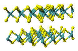
Layered structure of MoS
2, with Mo in blue and S in yellow Molybdenite-3D-balls.png
Layered structure of MoS
2
, with Mo in blue and S in yellow
Balls and sticks model of a single layer 1H and 1T molybdenum disulfide Balls and sticks model of a single layer 1H and 1T molybdenum disulfide.svg
Balls and sticks model of a single layer 1H and 1T molybdenum disulfide

Molybdenum disulfide monolayers consist of a unit of one layer of molybdenum atoms covalently bonded to two layers of sulfur atoms. While bulk molybdenum sulfide exists as 1T, 2H, or 3R polymorphs, molybdenum disulfide monolayers are found only in the 1T or 2H form. [96] The 2H form adopts a trigonal prismatic geometry [97] while the 1T form adopts an octahedral or trigonal antiprismatic geometry. [96] Molybdenum monolayers can also be stacked due to Van der Waals interactions between each layer.

Electrical

The electrical properties of molybdenum sulfide in electrical devices depends on factors such as the number of layers, [98] the synthesis method, [96] the nature of the substrate on which the monolayers are placed on, [99] and mechanical strain. [100]

As the number of layers decrease, the band gap begins to increase from 1.2eV in the bulk material up to a value of 1.9eV for a monolayer. [101] Odd number of molybdenum sulfide layers also produce different electrical properties than even numbers of molybdenum sulfide layers due to cyclic stretching and releasing present in the odd number of layers. [102] Molybdenum sulfide is a p-type material, but it shows ambipolar behavior when molybdenum sulfide monolayers that were 15 nm thick were used in transistors. [101] However, most electrical devices containing molybdenum sulfide monolayers tend to show n-type behavior. [97] [103]

The band gap of molybdenum disulfide monolayers can also be adjusted by applying mechanical strain [100] or an electrical field. [101] Increasing mechanical strain shifts the phonon modes of the molybdenum sulfide layers. [100] This results in a decrease of the band gap and metal-to-insulator transition. [96] Applying an electric field of 2-3Vnm−1 also decreases the indirect bandgap of molybdenum sulfide bilayers to zero. [96]

Solution phase lithium intercalation and exfoliation of bulk molybdenum sulfide produces molybdenum sulfide layers with metallic and semiconducting character due to the distribution of 1T and 2H geometries within the material. [101] [96] This is due to the two forms of molybdenum sulfide monolayers having different electrical properties. The 1T polymorph of molybdenum sulfide is metallic in character while the 2H form is more semiconducting. [97] However, molybdenum disulfide layers produced by electrochemical lithium intercalation are predominantly 1T and thus metallic in character as there is no conversion to the 2H form from the 1T form. [96]

Thermal

The thermal conductivity of molybdenum disulfide monolayers at room temperature is 34.5W/mK [104] while the thermal conductivity of few-layer molybdenum disulfide is 52W/mK. [104] The thermal conductivity of graphene, on the other hand, is 5300W/mK. [104] Due to the rather low thermal conductivity of molybdenum disulfide nanomaterials, it is not as promising material for high thermal applications as some other 2D materials.

Synthesis

[105]

Exfoliation

Exfoliation techniques for the isolating of molybdenum disulfide monolayers include mechanical exfoliation, [96] solvent assisted exfoliation, [97] and chemical exfoliation. [101]

Solvent assisted exfoliation is done by sonicating bulk molybdenum disulfide in an organic solvent such as isopropanol and N-methyl-2-pyrrolidone, which disperses the bulk material into nanosheets as the Van der Waals interactions between the layers in the bulk material are broken. [96] The amount of nanosheets produced is controlled by the sonication time, [97] the solvent-molybdenum disulfide interactions, [96] and the centrifuge speed. [96] Compared to other exfoliation techniques, solvent assisted exfoliation is the simplest method for large scale production of molybdenum disulfide nanosheets. [106]

The micromechanical exfoliation of molybdenum disulfide was inspired by the same technique used in the isolation of graphene nanosheets. [106] Micromechanical exfoliation allows for low defect molybdenum disulfide nanosheets but is not suitable for large scale production due to low yield. [97]

Chemical exfoliation involves functionalizing molybdenum difsulfide and then sonicating to disperse the nanosheets. [106] The most notable chemical exfoliation technique is lithium intercalation in which lithium is intercalated into bulk molybdenum disulfide and then dispersed into nanosheets by the addition of water. [101]

Chemical vapor deposition

Chemical vapor deposition of molybdenum disulfide nanosheets involves reacting molybdenum and sulfur precursors on a substrate at high temperatures. [106] This technique is often used in the preparing electrical devices with molybdenum disulfide components because the nanosheets are applied directly on the substrate; unfavorable interactions between the substrate and the nanosheets that would have occurred had they been separately synthesized are decreased. [97] In addition, since the thickness and area of the molybdenum disulfide nanosheets can be controlled by the selection of specific precursors, the electrical properties of the nanosheets can be tuned. [97]

Electroplating

Among the techniques that have been used to deposit molybdenum disulfide is electroplating. [107] Ultra-thin films consisting of few-layers have been produced via this technique over graphene electrodes. In addition, other electrode materials were also electroplated with MoS2, such as Titanium Nitride (TiN), glassy carbon and polytetrafluoroethylene. [108] [109] [110] The advantage that this technique offers in producing 2D materials is its spatial growth selectivity and its ability to deposit over 3D surfaces. Controlling the thickness of electrodeposited materials can be achieved by adjusting the deposition time or current.

Laser ablation

Pulsed laser deposition involves the thinning of bulk molybdenum disulfide by laser to produce single or multi-layer molybdenum disulfide nanosheets. [96] This allows for synthesis of molybdenum disulfide nanosheets with a defined shape and size. [101] The quality of the nanosheets are determined by the energy of the laser and the irradation angle. [106]

Lasers can also be used to form molybdenum disulfide nanosheets from molybdenum disulfide fullerene-like molecules. [111]

Hafnium disulfide

HfS
2 structure HfS2 structure.png
HfS
2
structure

Hafnium disulfide (HfS
2
) has a layered structure with strong covalent bonding between the Hf and S atoms in a layer and weak van der Waals forces between layers. The compound has CdI
2
type structure and is an indirect band gap semiconducting material. The interlayer spacing between the layers is 0.56 nm, which is small compared to group VIB TMDs like MoS
2
, making it difficult to cleave its atomic layers. However, recently its crystals with large interlayer spacing has grown using a chemical vapor transport route. [112] These crystals exfoliate in solvents like N-Cyclohexyl-2-pyrrolidone (CHP) in a time of just some minutes resulting in a high-yield production of its few-layers resulting in increase of its indirect bandgap from 0.9 eV to 1.3 eV. As an application in electronics, its field-effect transistors has been realised using its few layers as a conducting channel material offering a high current modulation ratio larger than 10000 at room temperature. Therefore, group IVB TMDs also holds potential applications in the field of opto-electronics.

Tungsten diselenide

Atomic image of a WSe2 monolayer showing hexagonal symmetry and three-fold defects. Scale bar: 2 nm (0.5 nm in the inset). WSe2 TEM.jpg
Atomic image of a WSe2 monolayer showing hexagonal symmetry and three-fold defects. Scale bar: 2 nm (0.5 nm in the inset).

Tungsten diselenide is an inorganic compound with the formula WSe
2
. The compound adopts a hexagonal crystalline structure similar to molybdenum disulfide. Every tungsten atom is covalently bonded to six selenium ligands in a trigonal prismatic coordination sphere, while each selenium is bonded to three tungsten atoms in a pyramidal geometry. The tungsten – selenium bond has a bond distance of 2.526 Å and the distance between selenium atoms is 3.34 Å. [113] Layers stack together via van der Waals interactions. WSe
2
is a stable semiconductor in the group-VI transition-metal dichalcogenides. The electronic bandgap of WSe
2
can be tuned by mechanical strain [114] which can also allow for conversion of the band type from indirect-to-direct in a WSe
2
bilayer. [115]

Related Research Articles

<span class="mw-page-title-main">Molybdenum disulfide</span> Chemical compound

Molybdenum disulfide is an inorganic compound composed of molybdenum and sulfur. Its chemical formula is MoS
2
.

<span class="mw-page-title-main">Graphene</span> Hexagonal lattice made of carbon atoms

Graphene is an allotrope of carbon consisting of a single layer of atoms arranged in a hexagonal lattice nanostructure. The name is derived from "graphite" and the suffix -ene, reflecting the fact that the graphite allotrope of carbon contains numerous double bonds.

<span class="mw-page-title-main">Phosphorene</span>

Phosphorene is a two-dimensional material consisting of phosphorus. It consists of a single layer of black phosphorus, the most stable allotrope of phosphorus. Phosphorene is analogous to graphene. Among two-dimensional materials, phosphorene is a competitor to graphene because it has a nonzero fundamental band gap that can be modulated by strain and the number of layers in a stack. Phosphorene was first isolated in 2014 by mechanical exfoliation. Liquid exfoliation is a promising method for scalable phosphorene production.

<span class="mw-page-title-main">Tungsten disulfide</span> Chemical compound

Tungsten disulfide is an inorganic chemical compound composed of tungsten and sulfur with the chemical formula WS2. This compound is part of the group of materials called the transition metal dichalcogenides. It occurs naturally as the rare mineral tungstenite. This material is a component of certain catalysts used for hydrodesulfurization and hydrodenitrification.

<span class="mw-page-title-main">Tantalum(IV) sulfide</span> Chemical compound

Tantalum(IV) sulfide is an inorganic compound with the formula TaS2. It is a layered compound with three-coordinate sulfide centres and trigonal prismatic or octahedral metal centres. It is structurally similar to molybdenum disulfide MoS2, and numerous other transition metal dichalcogenides. Tantalum disulfide has three polymorphs 1T-TaS2, 2H-TaS2, and 3R-TaS2, representing trigonal, hexagonal, and rhombohedral respectively.

<span class="mw-page-title-main">Molybdenum diselenide</span> Chemical compound

Molybdenum diselenide is an inorganic compound of molybdenum and selenium. Its structure is similar to that of MoS
2
. Compounds of this category are known as transition metal dichalcogenides, abbreviated TMDCs. These compounds, as the name suggests, are made up of a transition metals and elements of group 16 on the periodic table of the elements. Compared to MoS
2
, MoSe
2
exhibits higher electrical conductivity.

<span class="mw-page-title-main">Tungsten diselenide</span> Chemical compound

Tungsten diselenide is an inorganic compound with the formula WSe2. The compound adopts a hexagonal crystalline structure similar to molybdenum disulfide. The tungsten atoms are covalently bonded to six selenium ligands in a trigonal prismatic coordination sphere while each selenium is bonded to three tungsten atoms in a pyramidal geometry. The tungsten–selenium bond has a length of 0.2526 nm, and the distance between selenium atoms is 0.334 nm. It is a well studied example of a layered material. The layers stack together via van der Waals interactions. WSe2 is a very stable semiconductor in the group-VI transition metal dichalcogenides.

Valleytronics is an experimental area in semiconductors that exploits local extrema ("valleys") in the electronic band structure. Certain semiconductors have multiple "valleys" in the electronic band structure of the first Brillouin zone, and are known as multivalley semiconductors. Valleytronics is the technology of control over the valley degree of freedom, a local maximum/minimum on the valence/conduction band, of such multivalley semiconductors.

In materials science, the term single-layer materials or 2D materials refers to crystalline solids consisting of a single layer of atoms. These materials are promising for some applications but remain the focus of research. Single-layer materials derived from single elements generally carry the -ene suffix in their names, e.g. graphene. Single-layer materials that are compounds of two or more elements have -ane or -ide suffixes. 2D materials can generally be categorized as either 2D allotropes of various elements or as compounds.

A two-dimensional semiconductor is a type of natural semiconductor with thicknesses on the atomic scale. Geim and Novoselov et al. initiated the field in 2004 when they reported a new semiconducting material graphene, a flat monolayer of carbon atoms arranged in a 2D honeycomb lattice. A 2D monolayer semiconductor is significant because it exhibits stronger piezoelectric coupling than traditionally employed bulk forms. This coupling could enable applications. One research focus is on designing nanoelectronic components by the use of graphene as electrical conductor, hexagonal boron nitride as electrical insulator, and a transition metal dichalcogenide as semiconductor.

<span class="mw-page-title-main">Molybdenum ditelluride</span> Chemical compound

Molybdenum(IV) telluride, molybdenum ditelluride or just molybdenum telluride is a compound of molybdenum and tellurium with formula MoTe2, corresponding to a mass percentage of 27.32% molybdenum and 72.68% tellurium.

A rapidly increasing list of graphene production techniques have been developed to enable graphene's use in commercial applications.

Platinum diselenide is a transition metal dichalcogenide with the formula PtSe2. It is a layered substance that can be split into layers down to three atoms thick. PtSe2 can behave as a metalloid or as a semiconductor depending on the thickness.

<span class="mw-page-title-main">Boron nitride nanosheet</span>

Boron nitride nanosheet is a crystalline form of the hexagonal boron nitride (h-BN), which has a thickness of one atom. Similar in geometry as well as physical and thermal properties to its carbon analog graphene, but has very different chemical and electronic properties – contrary to the black and highly conducting graphene, BN nanosheets are electrical insulators with a band gap of ~5.9 eV, and therefore appear white in color.

<span class="mw-page-title-main">Hafnium disulfide</span> Chemical compound

Hafnium disulfide is an inorganic compound of hafnium and sulfur. It is a layered dichalcogenide with the chemical formula is HfS2. A few atomic layers of this material can be exfoliated using the standard Scotch Tape technique (see graphene) and used for the fabrication of a field-effect transistor. High-yield synthesis of HfS2 has also been demonstrated using liquid phase exfoliation, resulting in the production of stable few-layer HfS2 flakes. Hafnium disulfide powder can be produced by reacting hydrogen sulfide and hafnium oxides at 500–1300 °C.

Two dimensional hexagonal boron nitride is a material of comparable structure to graphene with potential applications in e.g. photonics., fuel cells and as a substrate for two-dimensional heterostructures. 2D h-BN is isostructural to graphene, but where graphene is conductive, 2D h-BN is a wide-gap insulator.

Tony Frederick Heinz is an American physicist.

<span class="mw-page-title-main">Layered materials</span>

In material science, layered materials are solids with highly anisotropic bonding, in which two-dimensional sheets are internally strongly bonded, but only weakly bonded to adjacent layers. Owing to their distinctive structures, layered materials are often suitable for intercalation reactions.

<span class="mw-page-title-main">Tantalum diselenide</span> Chemical compound

Tantalum diselenide is a compound made with tantalum and selenium atoms, with chemical formula TaSe2, which belongs to the family of transition metal dichalcogenides. In contrast to molybdenum disulfide (MoS2) or rhenium disulfide (ReS2), tantalum diselenide does not occur spontaneously in nature, but it can be synthesized. Depending on the growth parameters, different types of crystal structures can be stabilized.

First demonstrated in 2008, liquid-phase exfoliation (LPE) is a solution-processing method which is used to convert layered crystals into two-dimensional nanosheets in large quantities. It is currently one of the pillar methods for producing 2D nanosheets. According to IDTechEx, the family of exfoliation techniques which are directly or indirectly descended from LPE now make up over 60% of global graphene production capacity.

References

  1. 1 2 Eftekhari, A. (2017). "Tungsten dichalcogenides (WS2, WSe2, and WTe2): materials chemistry and applications". Journal of Materials Chemistry A. 5 (35): 18299–18325. doi:10.1039/C7TA04268J.
  2. 1 2 3 4 Splendiani, A.; Sun, L.; Zhang, Y.; Li, T.; Kim, J.; Chim, C. Y.; Galli, G.; Wang, F. (2010). "Emerging Photoluminescence in Monolayer MoS2". Nano Letters. 10 (4): 1271–5. Bibcode:2010NanoL..10.1271S. doi:10.1021/nl903868w. PMID   20229981.
  3. 1 2 3 Radisavljevic, B.; Radenovic, A.; Brivio, J.; Giacometti, V.; Kis, A. (2011). "Single-layer MoS2 transistors". Nature Nanotechnology. 6 (3): 147–50. Bibcode:2011NatNa...6..147R. doi:10.1038/nnano.2010.279. PMID   21278752.
  4. 1 2 Sundaram, R. S.; Engel, M.; Lombardo, A.; Krupke, R.; Ferrari, A. C.; Avouris, Ph; Steiner, M. (2013). "Electroluminescence in Single Layer MoS2". Nano Letters. 13 (4): 1416–1421. arXiv: 1211.4311 . Bibcode:2013NanoL..13.1416S. doi:10.1021/nl400516a. PMID   23514373. S2CID   207581247.
  5. 1 2 3 4 5 Lopez-Sanchez, O.; Lembke, D.; Kayci, M.; Radenovic, A.; Kis, A. (2013). "Ultrasensitive photodetectors based on monolayer MoS2". Nature Nanotechnology. 8 (7): 497–501. Bibcode:2013NatNa...8..497L. doi:10.1038/nnano.2013.100. PMID   23748194. S2CID   5435971.
  6. Rycerz, A.; Tworzydło, J.; Beenakker, C. W. J. (2007). "Valley filter and valley valve in graphene". Nature Physics. 3 (3): 172–175. arXiv: cond-mat/0608533 . Bibcode:2007NatPh...3..172R. doi:10.1038/nphys547. S2CID   119377206.
  7. 1 2 3 Cao, T.; Wang, G.; Han, W.; Ye, H.; Zhu, C.; Shi, J.; Niu, Q.; Tan, P.; Wang, E.; Liu, B.; Feng, J. (2012). "Valley-selective circular dichroism of monolayer molybdenum disulphide". Nature Communications. 3 (6): 887. arXiv: 1112.4013 . Bibcode:2012NatCo...3..887C. doi:10.1038/ncomms1882. PMC   3621397 . PMID   22673914.
  8. 1 2 Mak, K. F.; He, K.; Shan, J.; Heinz, T. F. (2012). "Control of valley polarization in monolayer MoS2 by optical helicity". Nature Nanotechnology. 7 (8): 494–8. arXiv: 1205.1822 . Bibcode:2012NatNa...7..494M. doi:10.1038/nnano.2012.96. PMID   22706698. S2CID   23248686.
  9. 1 2 3 Zeng, H.; Dai, J.; Yao, W.; Xiao, D.; Cui, X. (2012). "Valley polarization in MoS2 monolayers by optical pumping". Nature Nanotechnology. 7 (8): 490–3. arXiv: 1202.1592 . Bibcode:2012NatNa...7..490Z. doi:10.1038/nnano.2012.95. PMID   22706701. S2CID   13228054.
  10. Reyes-Retana, J.A.; Cervantes-Sodi, F. (2016). "Spin–orbital effects in metal-dichalcogenide semiconducting monolayers". Scientific Reports. 6: 24093. Bibcode:2016NatSR...624093R. doi:10.1038/srep24093. PMC   4837337 . PMID   27094967.
  11. Sallen, G.; Bouet, L.; Marie, X.; Wang, G.; Zhu, C.R.; Han, W.P.; Lu, P.; Tan, P.H.; Amand, T; Liu, B.L.; Urbaszek, B. (2012). "Robust optical emission polarization in MoS2 monolayers through selective valley excitation". Physical Review B. 86 (8): 3–6. arXiv: 1206.5128 . Bibcode:2012PhRvB..86h1301S. doi:10.1103/PhysRevB.86.081301. S2CID   62890713.
  12. Husain, Sajid; Kumar, Abhishek; Kumar, Prabhat; Kumar, Ankit; Barwal, Vineet; Behera, Nilamani; Choudhary, Sudhanshu; Svedlindh, Peter; Chaudhary, Sujeet (2018). "Spin pumping in the Heusler alloy Co2FeAl/MoS2 heterostructure: Ferromagnetic resonance experiment and theory". Physical Review B. 98 (18): 180404. Bibcode:2018PhRvB..98r0404H. doi:10.1103/PhysRevB.98.180404. S2CID   125218447.
  13. Husain, Sajid; Gupta, Rahul; Kumar, Ankit; Kumar, Prabhat; Behera, Nilamani; Brucas, Rimantas; Chaudhary, Sujeet; Svedlindh, Peter (2020-12-01). "Emergence of spin–orbit torques in 2D transition metal dichalcogenides: A status update". Applied Physics Reviews. 7 (4): 041312. Bibcode:2020ApPRv...7d1312H. doi:10.1063/5.0025318. S2CID   230546779.
  14. Briggs, Natalie; Subramanian, Shruti; Lin, Zhong; Li, Xufan; Zhang, Xiaotian; Zhang, Kehao; Xiao, Kai; Geohegan, David; Wallace, Robert; Chen, Long-Qing; Terrones, Mauricio; Ebrahimi, Aida; Das, Saptarshi; Redwing, Joan; Hinkle, Christopher; Momeni, Kasra; van Duin, Adri; Crespi, Vin; Kar, Swastik; Robinson, Joshua A. (2019). "A roadmap for electronic grade 2D materials". 2D Materials. 6 (2): 022001. Bibcode:2019TDM.....6b2001B. doi:10.1088/2053-1583/aaf836. OSTI   1503991. S2CID   188118830.
  15. "2-D materials enhance a 3-D world". phys.org. 2017-01-10.
  16. Nealon, Cory (2016-05-13). "This 'nanocavity' may improve ultrathin solar panels, video cameras and more". phys.org.
  17. Sung, S.H.; Schnitzer, N.; Brown, L.; Park, J.; Hovden, R. (2019). "Stacking, strain, and twist in 2D materials quantified by 3D electron diffraction". Physical Review Materials. 3 (6): 064003. arXiv: 1905.11354 . Bibcode:2019PhRvM...3f4003S. doi:10.1103/PhysRevMaterials.3.064003. S2CID   166228311.
  18. Kumar, N.; Najmaei, S.; Cui, Q.; Ceballos, F.; Ajayan, P.; Lou, J.; Zhao, H. (2013). "Second harmonic microscopy of monolayer MoS2". Physical Review B. 87 (16): 161403. arXiv: 1302.3935 . Bibcode:2013PhRvB..87p1403K. doi:10.1103/PhysRevB.87.161403. S2CID   1796583.
  19. Malard, L. M.; Alencar, T. V.; Barboza, A. P. M.; Mak, K. F.; De Paula, A. M. (2013). "Observation of intense second harmonic generation from MoS2 atomic crystals". Physical Review B. 87 (20): 201401. arXiv: 1304.4289 . Bibcode:2013PhRvB..87t1401M. doi:10.1103/PhysRevB.87.201401. S2CID   118392637.
  20. Zeng, H.; Liu, G. B.; Dai, J.; Yan, Y.; Zhu, B.; He, R.; Xie, L.; Xu, S.; Chen, X.; Yao, W.; Cui, X. (2013). "Optical signature of symmetry variations and spin-valley coupling in atomically thin tungsten dichalcogenides". Scientific Reports. 3: 1608. arXiv: 1208.5864 . Bibcode:2013NatSR...3E1608Z. doi:10.1038/srep01608. PMC   3622914 . PMID   23575911.
  21. 1 2 3 Wang, G.; Marie, X.; Gerber, I.; Amand, T.; Lagarde, D.; Bouet, L.; Vidal, M.; Balocchi, A.; Urbaszek, B. (2015). "Giant Enhancement of the Optical Second-Harmonic Emission of WSe2 Monolayers by Laser Excitation at Exciton Resonances". Physical Review Letters. 114 (9): 097403. arXiv: 1404.0056 . Bibcode:2015PhRvL.114i7403W. doi:10.1103/PhysRevLett.114.097403. PMID   25793850. S2CID   119247783.
  22. 1 2 Xiao, D.; Liu, G. B.; Feng, W.; Xu, X.; Yao, W. (2012). "Coupled Spin and Valley Physics in Monolayers of MoS2 and Other Group-VI Dichalcogenides". Physical Review Letters. 108 (19): 196802. arXiv: 1112.3144 . Bibcode:2012PhRvL.108s6802X. doi:10.1103/PhysRevLett.108.196802. PMID   23003071. S2CID   13621082.
  23. Jones, A. M.; Yu, H.; Ghimire, N. J.; Wu, S.; Aivazian, G.; Ross, J. S.; Zhao, B.; Yan, J.; Mandrus, D. G.; Xiao, D.; Yao, W.; Xu, X. (2013). "Optical generation of excitonic valley coherence in monolayer WSe2". Nature Nanotechnology. 8 (9): 634–8. arXiv: 1303.5318 . Bibcode:2013NatNa...8..634J. doi:10.1038/nnano.2013.151. PMID   23934096. S2CID   7090218.
  24. Xu, X.; Yao, W.; Xiao, D.; Heinz, T. F. (2014). "Spin and pseudospins in layered transition metal dichalcogenides". Nature Physics. 10 (5): 343–350. Bibcode:2014NatPh..10..343X. doi:10.1038/nphys2942. S2CID   85510443.
  25. Manzeli, Sajedeh; Ovchinnikov, Dmitry; Pasquier, Diego; Yazyev, Oleg V.; Kis, Andras (2017-06-13). "2D transition metal dichalcogenides". Nature Reviews Materials. 2 (8): 17033. Bibcode:2017NatRM...217033M. doi:10.1038/natrevmats.2017.33. ISSN   2058-8437.
  26. Ramasubramaniam, A. (2012). "Large excitonic effects in monolayers of molybdenum and tungsten dichalcogenides". Physical Review B. 86 (11): 115409. Bibcode:2012PhRvB..86k5409R. doi:10.1103/PhysRevB.86.115409.
  27. 1 2 Qiu, D. Y.; Da Jornada, F. H.; Louie, S. G. (2013). "Optical Spectrum of MoS2: Many-Body Effects and Diversity of Exciton States". Physical Review Letters. 111 (21): 216805. arXiv: 1311.0963 . Bibcode:2013PhRvL.111u6805Q. doi:10.1103/PhysRevLett.111.216805. PMID   24313514. S2CID   19063715.
  28. Strauß, Fabian; Kohlschreiber, Pia; Keck, Jakob; Michel, Patrick; Hiller, Jonas; Meixner, Alfred J.; Scheele, Marcus (2024). "A simple 230 MHz photodetector based on exfoliated WSe 2 multilayers". RSC Applied Interfaces. doi: 10.1039/D4LF00019F .
  29. Akinwande, Deji; Petrone, Nicholas; Hone, James (2014-12-17). "Two-dimensional flexible nanoelectronics". Nature Communications. 5: 5678. Bibcode:2014NatCo...5.5678A. doi: 10.1038/ncomms6678 . PMID   25517105.
  30. Lee, Changgu; Wei, Xiaoding; Kysar, Jeffrey W.; Hone, James (2008-07-18). "Measurement of the Elastic Properties and Intrinsic Strength of Monolayer Graphene". Science. 321 (5887): 385–388. Bibcode:2008Sci...321..385L. doi:10.1126/science.1157996. PMID   18635798. S2CID   206512830.
  31. 1 2 Bertolazzi, Simone; Brivio, Jacopo; Kis, Andras (2011-11-16). "Stretching and Breaking of Ultrathin MoS2". ACS Nano. 5 (12): 9703–9709. doi:10.1021/nn203879f. PMID   22087740.
  32. Castellanos-Gomez, Andres; Poot, Menno; Steele, Gary A.; van der Zant, Herre S. J.; Agraït, Nicolás; Rubio-Bollinger, Gabino (2012). "Elastic Properties of Freely Suspended MoS2 Nanosheets". Advanced Materials. 24 (6): 772–775. arXiv: 1202.4439 . Bibcode:2012AdM....24..772C. doi:10.1002/adma.201103965. PMID   22231284. S2CID   205243099.
  33. Zhang, Rui; Koutsos, Vasileious; Cheung, Cheung (January 2016). "Elastic properties of suspended multilayer WSe2". Applied Physics Letters. 108 (4): 042104. Bibcode:2016ApPhL.108d2104Z. doi: 10.1063/1.4940982 . hdl: 20.500.11820/a69c599d-0b00-4fd5-80bd-1b1493ce56e1 .
  34. 1 2 Liu, Kai; Yan, Qimin; Chen, Michelle; Fan, Wen; Sun, Yinghui; Suh, Joonki; Fu, Deyi; Lee, Sangwook; Zhou, Jian (2014). "Elastic Properties of Chemical-Vapor-Deposited Monolayer MoS2, WS2, and Their Bilayer Heterostructures". Nano Letters. 14 (9): 5097–5103. arXiv: 1407.2669 . Bibcode:2014NanoL..14.5097L. doi:10.1021/nl501793a. PMID   25120033. S2CID   2136100.
  35. He, K.; Poole, C.; Mak, K. F.; Shan, J. (2013). "Experimental Demonstration of Continuous Electronic Structure Tuning via Strain in Atomically Thin MoS2". Nano Letters. 13 (6): 2931–6. arXiv: 1305.3673 . Bibcode:2013NanoL..13.2931H. doi:10.1021/nl4013166. PMID   23675872. S2CID   207691793.
  36. Conley, H. J.; Wang, B.; Ziegler, J. I.; Haglund, R. F.; Pantelides, S. T.; Bolotin, K. I. (2013). "Bandgap Engineering of Strained Monolayer and Bilayer MoS2". Nano Letters. 13 (8): 3626–30. arXiv: 1305.3880 . Bibcode:2013NanoL..13.3626C. doi:10.1021/nl4014748. PMID   23819588. S2CID   8191142.
  37. Zhu, C. R.; Wang, G.; Liu, B. L.; Marie, X.; Qiao, X. F.; Zhang, X.; Wu, X. X.; Fan, H.; Tan, P. H.; Amand, T.; Urbaszek, B. (2013). "Strain tuning of optical emission energy and polarization in monolayer and bilayer MoS2". Physical Review B. 88 (12): 121301. arXiv: 1306.3442 . Bibcode:2013PhRvB..88l1301Z. doi:10.1103/PhysRevB.88.121301. S2CID   119269184.
  38. 1 2 Novoselov, K. S.; Jiang, D; Schedin, F; Booth, T. J.; Khotkevich, V. V.; Morozov, S. V.; Geim, A. K. (2005). "Two-dimensional atomic crystals". Proceedings of the National Academy of Sciences. 102 (30): 10451–3. arXiv: cond-mat/0503533 . Bibcode:2005PNAS..10210451N. doi: 10.1073/pnas.0502848102 . PMC   1180777 . PMID   16027370.
  39. Coleman, Jonathan N.; Lotya, Mustafa; O’Neill, Arlene; Bergin, Shane D.; King, Paul J.; Khan, Umar; Young, Karen; Gaucher, Alexandre; De, Sukanta; Smith, Ronan J.; Shvets, Igor V.; Arora, Sunil K.; Stanton, George; Kim, Hye-Young; Lee, Kangho; Kim, Gyu Tae; Duesberg, Georg S.; Hallam, Toby; Boland, John J.; Wang, Jing Jing; Donegan, John F.; Grunlan, Jaime C.; Moriarty, Gregory; Shmeliov, Aleksey; Nicholls, Rebecca J.; Perkins, James M.; Grieveson, Eleanor M.; Theuwissen, Koenraad; McComb, David W.; Nellist, Peter D.; Nicolosi, Valeria (2011). "Two-Dimensional Nanosheets Produced by Liquid Exfoliation of Layered Materials". Science. 331 (6017): 568–571. Bibcode:2011Sci...331..568C. doi:10.1126/science.1194975. hdl: 2262/66458 . PMID   21292974. S2CID   23576676.
  40. Zhou, Jiadong; Lin, Junhao; Huang, Xiangwei; Zhou, Yao; Chen, Yu; Xia, Juan; Wang, Hong; Xie, Yu; Yu, Huimei; Lei, Jincheng; Wu, Di; Liu, Fucai; Fu, Qundong; Zeng, Qingsheng; Hsu, Chuang-Han (2018). "A library of atomically thin metal chalcogenides". Nature. 556 (7701): 355–359. Bibcode:2018Natur.556..355Z. doi:10.1038/s41586-018-0008-3. hdl: 10356/84198 . ISSN   1476-4687. PMID   29670263. S2CID   4945645.{{cite journal}}: CS1 maint: date and year (link)
  41. 1 2 3 Kim, Se-Yang; Kwak, Jinsung; Ciobanu, Cristian V.; Kwon, Soon-Yong (February 2019). "Recent Developments in Controlled Vapor-Phase Growth of 2D Group 6 Transition Metal Dichalcogenides". Advanced Materials. 31 (20): 1804939. Bibcode:2019AdM....3104939K. doi: 10.1002/adma.201804939 . ISSN   0935-9648. PMID   30706541.
  42. Shi, Yumeng; Li, Henan; Li, Lain-Jong (2015-04-28). "Recent advances in controlled synthesis of two-dimensional transition metal dichalcogenides via vapour deposition techniques". Chemical Society Reviews. 44 (9): 2744–2756. doi:10.1039/C4CS00256C. ISSN   1460-4744. PMID   25327436.
  43. "AIXTRON Technologies: MOCVD :: AIXTRON". www.aixtron.com. Retrieved 2019-12-02.
  44. Lee, Y. H.; Zhang, X. Q.; Zhang, W; Chang, M. T.; Lin, C. T.; Chang, K. D.; Yu, Y. C.; Wang, J. T.; Chang, C. S.; Li, L. J.; Lin, T. W. (2012). "Synthesis of large-area MoS2 atomic layers with chemical vapor deposition". Advanced Materials. 24 (17): 2320–5. arXiv: 1202.5458 . Bibcode:2012AdM....24.2320L. doi:10.1002/adma.201104798. PMID   22467187. S2CID   11713759.
  45. Kim, Ki Seok; Lee, Doyoon; Chang, Celesta S.; Seo, Seunghwan; Hu, Yaoqiao; Cha, Soonyoung; Kim, Hyunseok; Shin, Jiho; Lee, Ju-Hee; Lee, Sangho; Kim, Justin S.; Kim, Ki Hyun; Suh, Jun Min; Meng, Yuan; Park, Bo-In (2023-01-18). "Non-epitaxial single-crystal 2D material growth by geometric confinement". Nature. 614 (7946): 88–94. Bibcode:2023Natur.614...88K. doi:10.1038/s41586-022-05524-0. ISSN   1476-4687. PMID   36653458. S2CID   255970742.
  46. 1 2 3 4 5 6 Wei, Y; Hu, C; Li, Y; Hu, X; Yu, K; Su, L (Jul 2020). "Initial stage of MBE growth of MoSe2 monolayer". Nanotechnology. 31 (31): 315710. Bibcode:2020Nanot..31E5710W. doi:10.1088/1361-6528/ab884b. PMID   32272461. S2CID   215727487 . Retrieved 21 July 2022.
  47. 1 2 Lasek, K; Coelho, P. M; Zberecki, K; Xin, Y; Kolekar, S. K; Li, J; Batzill, M (25 June 2020). "Molecular Beam Epitaxy of Transition Metal (Ti-, V-, and Cr-) Tellurides: From Monolayer Ditellurides to Multilayer Self-Intercalation Compounds". ACS Nano. 14 (7): 8473–8484. doi:10.1021/acsnano.0c02712. PMID   32584543. S2CID   220074214 . Retrieved 21 July 2022.
  48. 1 2 3 4 Nakano, M; Wang, Y; Kashiwabara, Y; Matsuoka, H; Iwasa, Y (2017). "Layer-by-Layer Epitaxial Growth of Scalable WSe2 on Sapphire by Molecular Beam Epitaxy". Nano Letters. 17 (9): 5595–5599. arXiv: 1709.02912 . Bibcode:2017NanoL..17.5595N. doi:10.1021/acs.nanolett.7b02420. PMID   28849935. S2CID   206742437 . Retrieved 21 July 2022.
  49. Hall, Joshua; Pielic, Borna; Murray, Clifford; Jolie, Wouter; Wekking, Tobias; Busse, Carsten; Kralj, Marko; Michley, Thomas (2018). "Molecular beam epitaxy of quasi-freestanding transition metal disulphide monolayers on van der Waals substrates: a growth study". 2D Mater. 5 (2): 025005. Bibcode:2018TDM.....5b5005H. doi:10.1088/2053-1583/aaa1c5. S2CID   103289660 . Retrieved 28 November 2022.
  50. Choudury, TH; Zhang, X; Balushi, ZY AL; Chubarov, M; Redwing, JM (Jul 2020). "Epitaxial Growth of Two-Dimensional Layered Transition Metal Dichalcogenides". Annual Review of Materials Research. 50: 155–177. arXiv: 1909.03502 . Bibcode:2020AnRMS..50..155C. doi:10.1146/annurev-matsci-090519-113456. S2CID   202540441 . Retrieved 21 July 2022.
  51. 1 2 Singh, D. K; Gupta, G (2022). "van der Waals Epitaxy of Transition Metal Dichalcogenides via Molecular Beam Epitaxy: Looking Back and Moving Forward". Materials Advances. 3 (15): 6142–6156. doi: 10.1039/D2MA00352J . S2CID   250156491.
  52. Noori, Y J; Thomas, S; Ramadan, S; Greenacre, V K; Abdelazim, N M; Han, Y; Zhang, J; Beanland, R; Hector, A L; Klein, N; Reid, G; Bartlett, P N; de Groot, C H (2022-01-01). "Electrodeposited WS 2 monolayers on patterned graphene". 2D Materials. 9 (1): 015025. arXiv: 2109.00083 . Bibcode:2022TDM.....9a5025N. doi:10.1088/2053-1583/ac3dd6. ISSN   2053-1583. S2CID   244693600.
  53. Noori, Yasir J.; Thomas, Shibin; Ramadan, Sami; Smith, Danielle E.; Greenacre, Vicki K.; Abdelazim, Nema; Han, Yisong; Beanland, Richard; Hector, Andrew L.; Klein, Norbert; Reid, Gillian; Bartlett, Philip N.; Kees de Groot, C. H. (2020-11-04). "Large-Area Electrodeposition of Few-Layer MoS 2 on Graphene for 2D Material Heterostructures". ACS Applied Materials & Interfaces. 12 (44): 49786–49794. arXiv: 2005.08616 . doi:10.1021/acsami.0c14777. ISSN   1944-8244. PMID   33079533. S2CID   224828493.
  54. Wan, Xi; Chen, Kun; Chen, Zefeng; Xie, Fangyan; Zeng, Xiaoliang; Xie, Weiguang; Chen, Jian; Xu, Jianbin (May 2017). "Controlled Electrochemical Deposition of Large-Area MoS 2 on Graphene for High-Responsivity Photodetectors". Advanced Functional Materials. 27 (19): 1603998. doi:10.1002/adfm.201603998. S2CID   100120486.
  55. Thomas, Shibin; Smith, Danielle E.; Greenacre, Victoria K.; Noori, Yasir J.; Hector, Andrew L.; Groot, C. H. (Kees) de; Reid, Gillian; Bartlett, Philip N. (2020-01-06). "Electrodeposition of MoS2 from Dichloromethane". Journal of the Electrochemical Society. 167 (10): 106511. Bibcode:2020JElS..167j6511T. doi: 10.1149/1945-7111/ab9c88 . ISSN   0013-4651. S2CID   225720683.
  56. Abdelazim, Nema M.; Noori, Yasir J.; Thomas, Shibin; Greenacre, Victoria K.; Han, Yisong; Smith, Danielle E.; Piana, Giacomo; Zhelev, Nikolay; Hector, Andrew L.; Beanland, Richard; Reid, Gillian; Bartlett, Philip N.; Groot, Cornelis H. (September 2021). "Lateral Growth of MoS 2 2D Material Semiconductors Over an Insulator Via Electrodeposition". Advanced Electronic Materials. 7 (9): 2100419. doi: 10.1002/aelm.202100419 . ISSN   2199-160X. S2CID   232478824.
  57. Mak, K. F.; Lee, C.; Hone, J.; Shan, J.; Heinz, T. F. (2010). "Atomically Thin MoS2: A New Direct-Gap Semiconductor". Physical Review Letters. 105 (13): 136805. arXiv: 1004.0546 . Bibcode:2010PhRvL.105m6805M. doi:10.1103/PhysRevLett.105.136805. PMID   21230799. S2CID   40589037.
  58. Cheng, Y. C.; Zhu, Z. Y.; Tahir, M.; Schwingenschlogl, U. (2012). "Spin–orbit–induced spin splittings in polar transition metal dichalcogenide monolayers". EPL. 102 (5): 57001. Bibcode:2013EL....10257001C. doi:10.1209/0295-5075/102/57001. S2CID   121978058.
  59. 1 2 Liu, G. B.; Shan, W. Y.; Yao, Y.; Yao, W.; Xiao, D. (2013). "Three-band tight-binding model for monolayers of group-VIB transition metal dichalcogenides". Physical Review B. 88 (8): 085433. arXiv: 1305.6089 . Bibcode:2013PhRvB..88h5433L. doi:10.1103/PhysRevB.88.085433. S2CID   119111681.
  60. Zhu, Z.; Cheng, Y. C.; Schwingenschlogl, U. (2011). "Giant spin–orbit-induced spin splitting in two-dimensional transition-metal dichalcogenide semiconductors". Physical Review B. 84 (15): 153402. Bibcode:2011PhRvB..84o3402Z. doi:10.1103/PhysRevB.84.153402. hdl: 10754/315771 .
  61. Kośmider, K.; González, J. W.; Fernández-Rossier, J. (2013). "Large spin splitting in the conduction band of transition metal dichalcogenide monolayers". Physical Review B. 88 (24): 245436. arXiv: 1311.0049 . Bibcode:2013PhRvB..88x5436K. doi:10.1103/PhysRevB.88.245436. S2CID   31176688.
  62. Kormányos, A.; Zólyomi, V.; Drummond, N. D.; Burkard, G. (2014). "Spin–Orbit Coupling, Quantum Dots, and Qubits in Monolayer Transition Metal Dichalcogenides". Physical Review X. 4 (1): 011034. arXiv: 1310.7720 . Bibcode:2014PhRvX...4a1034K. doi:10.1103/PhysRevX.4.011034. S2CID   17909293.
  63. Bussolotti, Fabio; Kawai, Hiroyo; Ooi, Zi En; Chellappan, Vijila; Thian, Dickson; Pang, Ai Lin Christina; Goh, Kuan Eng Johnson (2018). "Roadmap on finding chiral valleys: screening 2D materials for valleytronics". Nano Futures. 2 (3): 032001. Bibcode:2018NanoF...2c2001B. doi:10.1088/2399-1984/aac9d7. S2CID   139826293.
  64. 1 2 Chernikov, Alexey; Berkelbach, Timothy C.; Hill, Heather M.; Rigosi, Albert; Li, Yilei; Aslan, Ozgur Burak; Reichman, David R.; Hybertsen, Mark S.; Heinz, Tony F. (2014). "Exciton Binding Energy and Nonhydrogenic Rydberg Series in Monolayer WS2". Physical Review Letters. 113 (7): 076802. arXiv: 1403.4270 . Bibcode:2014PhRvL.113g6802C. doi:10.1103/PhysRevLett.113.076802. PMID   25170725. S2CID   23157872.
  65. Ye, Ziliang; Cao, Ting; O’Brien, Kevin; Zhu, Hanyu; Yin, Xiaobo; Wang, Yuan; Louie, Steven G.; Zhang, Xiang (2014). "Probing excitonic dark states in single-layer tungsten disulphide". Nature. 513 (7517): 214–218. arXiv: 1403.5568 . Bibcode:2014Natur.513..214Y. doi:10.1038/nature13734. PMID   25162523. S2CID   4461357.
  66. Ugeda, M. M.; Bradley, A. J.; Shi, S. F.; Da Jornada, F. H.; Zhang, Y.; Qiu, D. Y.; Ruan, W.; Mo, S. K.; Hussain, Z.; Shen, Z. X.; Wang, F.; Louie, S. G.; Crommie, M. F. (2014). "Giant bandgap renormalization and excitonic effects in a monolayer transition metal dichalcogenide semiconductor". Nature Materials. 13 (12): 1091–1095. arXiv: 1404.2331 . Bibcode:2014NatMa..13.1091U. doi:10.1038/nmat4061. PMID   25173579. S2CID   25491405.
  67. 1 2 Manca, M.; Glazov, M. M.; Robert, C.; Cadiz, F.; Taniguchi, T.; Watanabe, K.; Courtade, E.; Amand, T.; Renucci, P.; Marie, X.; Wang, G.; Urbaszek, B. (2017). "Enabling valley selective exciton scattering in monolayer WSe2 through upconversion". Nat. Commun. 8: 14927. arXiv: 1701.05800 . Bibcode:2017NatCo...814927M. doi:10.1038/ncomms14927. PMC   5382264 . PMID   28367962.
  68. Ross, J. S.; et al. (2013). "Electrical control of neutral and charged excitons in a monolayer semiconductor". Nat. Commun. 4: 1474. arXiv: 1211.0072 . Bibcode:2013NatCo...4.1474R. doi:10.1038/ncomms2498. PMID   23403575. S2CID   9872370.
  69. Mak, K. F.; et al. (2013). "Tightly bound trions in monolayer MoS2". Nat. Mater. 12 (3): 207–211. arXiv: 1210.8226 . Bibcode:2013NatMa..12..207M. doi:10.1038/nmat3505. PMID   23202371. S2CID   205408065.
  70. Cadiz, F.; Courtade, E.; Robert, C.; Wang, G.; Shen, Y.; Cai, H.; Taniguchi, T.; Watanabe, K.; Carrere, H.; Lagarde, D.; Manca, M.; Amand, T.; Renucci, P.; Tongay, S.; Marie, X.; Urbaszek, B. (2017). "Excitonic linewidth approaching the homogeneous limit in MoS2 based van der Waals heterostructures : accessing spin-valley dynamics". Physical Review X. 7 (2): 021026. arXiv: 1702.00323 . Bibcode:2017PhRvX...7b1026C. doi:10.1103/PhysRevX.7.021026. S2CID   55508192.
  71. Mai, C.; et al. (2014). "Many-Body Effects in Valleytronics: Direct Measurement of Valley Lifetimes in Single-Layer MoS2". Nano Lett. 14 (1): 202–206. Bibcode:2014NanoL..14..202M. doi:10.1021/nl403742j. PMID   24325650.
  72. Shang, J.; et al. (2015). "Observation of Excitonic Fine Structure in a 2D Transition-Metal Dichalcogenide Semiconductor". ACS Nano. 9 (1): 647–655. doi:10.1021/nn5059908. PMID   25560634.
  73. Mostaani, E.; et al. (2017). "Diffusion quantum Monte Carlo study of excitonic complexes in two-dimensional transition-metal dichalcogenides". Physical Review B. 96 (7): 075431. arXiv: 1706.04688 . Bibcode:2017PhRvB..96g5431M. doi:10.1103/PhysRevB.96.075431. S2CID   46144082.
  74. Kern, Johannes; Niehues, Iris; Tonndorf, Philipp; Schmidt, Robert; Wigger, Daniel; Schneider, Robert; Stiehm, Torsten; Michaelis de Vasconcellos, Steffen; Reiter, Doris E. (September 2016). "Nanoscale Positioning of Single-Photon Emitters in Atomically Thin WSe2". Advanced Materials. 28 (33): 7101–7105. Bibcode:2016AdM....28.7101K. doi:10.1002/adma.201600560. PMID   27305430. S2CID   205268567.
  75. He, Yu-Ming; Clark, Genevieve; Schaibley, John R.; He, Yu; Chen, Ming-Cheng; Wei, Yu-Jia; Ding, Xing; Zhang, Qiang; Yao, Wang (2015). "Single quantum emitters in monolayer semiconductors". Nature Nanotechnology. 10 (6): 497–502. arXiv: 1411.2449 . Bibcode:2015NatNa..10..497H. doi:10.1038/nnano.2015.75. PMID   25938571. S2CID   205454184.
  76. Palacios-Berraquero, Carmen; Kara, Dhiren M.; Montblanch, Alejandro R.-P.; Barbone, Matteo; Latawiec, Pawel; Yoon, Duhee; Ott, Anna K.; Loncar, Marko; Ferrari, Andrea C. (August 2017). "Large-scale quantum-emitter arrays in atomically thin semiconductors". Nature Communications. 8 (1): 15093. arXiv: 1609.04244 . Bibcode:2017NatCo...815093P. doi:10.1038/ncomms15093. PMC   5458119 . PMID   28530249.
  77. Palacios-Berraquero, Carmen; Barbone, Matteo; Kara, Dhiren M.; Chen, Xiaolong; Goykhman, Ilya; Yoon, Duhee; Ott, Anna K.; Beitner, Jan; Watanabe, Kenji (December 2016). "Atomically thin quantum light-emitting diodes". Nature Communications. 7 (1): 12978. arXiv: 1603.08795 . Bibcode:2016NatCo...712978P. doi:10.1038/ncomms12978. PMC   5052681 . PMID   27667022.
  78. Wu, Wei; Dass, Chandriker K.; Hendrickson, Joshua R.; Montaño, Raul D.; Fischer, Robert E.; Zhang, Xiaotian; Choudhury, Tanushree H.; Redwing, Joan M.; Wang, Yongqiang (2019). "Locally defined quantum emission from epitaxial few-layer tungsten diselenide". Applied Physics Letters. 114 (21): 213102. Bibcode:2019ApPhL.114u3102W. doi: 10.1063/1.5091779 . hdl: 10150/634575 .
  79. Dass, Chandriker Kavir; Khan, Mahtab A.; Clark, Genevieve; Simon, Jeffrey A.; Gibson, Ricky; Mou, Shin; Xu, Xiaodong; Leuenberger, Michael N.; Hendrickson, Joshua R. (2019). "Ultra-Long Lifetimes of Single Quantum Emitters in Monolayer WSe2/hBN Heterostructures". Advanced Quantum Technologies. 2 (5–6): 1900022. doi: 10.1002/qute.201900022 .
  80. Srour, J.R.; McGarity, J.M. (1988). "Radiation effects on microelectronics in space". Proc. IEEE. 76 (11): 1443–1469. doi:10.1109/5.90114.
  81. Walker, R.C.; Shi, T. (2016). "Radiation effects on two-dimensional materials". Proc. Physical Status Solida.
  82. Freitag, M.; Low, T.; Avouris, P. (2013). "Increased responsivity of suspended graphene photodetectors". Nano Letters. 13 (4): 1644–1648. Bibcode:2013NanoL..13.1644F. doi:10.1021/nl4001037. PMID   23452264.
  83. Lee, H.S. (2012). "MoS2 nanosheet phototransistors with thickness-modulated optical energy gap". Nano Letters. 12 (7): 3695–3700. Bibcode:2012NanoL..12.3695L. doi:10.1021/nl301485q. PMID   22681413.
  84. Liu, F.; Shimotani, H.; Shang, H. (2014). "High-sensitivity photodetectors based on multilayer GaTe flakes". ACS Nano. 8 (1): 752–760. doi:10.1021/nn4054039. PMID   24364508.
  85. 1 2 Lu, Ang-Yu; Zhu, Hanyu; Xiao, Jun; Chuu, Chih-Piao; Han, Yimo; Chiu, Ming-Hui; Cheng, Chia-Chin; Yang, Chih-Wen; Wei, Kung-Hwa; Yang, Yiming; Wang, Yuan; Sokaras, Dimosthenis; Nordlund, Dennis; Yang, Peidong; Muller, David A.; Chou, Mei-Yin; Zhang, Xiang; Li, Lain-Jong (2017). "Janus monolayers of transition metal dichalcogenides". Nature Nanotechnology. 12 (8): 744–749. doi:10.1038/nnano.2017.100. PMID   28507333. S2CID   42620382.
  86. Cheng, Y. C.; Zhu, Z. Y.; Tahir, M.; Schwingenschlögl, U. (2013). "Spin–orbit–induced spin splittings in polar transition metal dichalcogenide monolayers". EPL (Europhysics Letters). 102 (5): 57001. Bibcode:2013EL....10257001C. doi:10.1209/0295-5075/102/57001. S2CID   121978058.
  87. Li, Fengping; Wei, Wei; Zhao, Pei; Huang, Baibiao; Dai, Ying (2017). "Electronic and Optical Properties of Pristine and Vertical and Lateral Heterostructures of Janus MoSSe and WSSe". The Journal of Physical Chemistry Letters. 8 (23): 5959–5965. doi:10.1021/acs.jpclett.7b02841. PMID   29169238.
  88. Dong, Liang; Lou, Jun; Shenoy, Vivek B. (2017). "Large In-Plane and Vertical Piezoelectricity in Janus Transition Metal Dichalchogenides[sic]". ACS Nano. 11 (8): 8242–8248. doi:10.1021/acsnano.7b03313. PMID   28700210.
  89. Zhang, Jing; Jia, Shuai; Kholmanov, Iskandar; Dong, Liang; Er, Dequan; Chen, Weibing; Guo, Hua; Jin, Zehua; Shenoy, Vivek B. (2017). "Janus Monolayer Transition-Metal Dichalcogenides". ACS Nano. 11 (8): 8192–8198. arXiv: 1704.06389 . doi:10.1021/acsnano.7b03186. PMID   28771310. S2CID   31445401.
  90. Ma, Xiangchao; Wu, Xin; Wang, Haoda; Wang, Yucheng (2018). "A Janus MoSSe monolayer: a potential wide solar-spectrum water-splitting photocatalyst with a low carrier recombination rate". Journal of Materials Chemistry A. 6 (5): 2295–2301. doi:10.1039/c7ta10015a.
  91. Radisavljevic, B.; Radenovic, A.; Brivio, J.; Giacometti, V.; Kis, A. (2011). "Single-layer MoS2 transistors". Nature Nanotechnology. 6 (3): 147–50. Bibcode:2011NatNa...6..147R. doi:10.1038/nnano.2010.279. PMID   21278752.
  92. Choi, Wonbong; Choudhary, Nitin; Han, Gang Hee; Park, Juhong; Akinwande, Deji; Lee, Young Hee (2017-04-01). "Recent development of two-dimensional transition metal dichalcogenides and their applications". Materials Today. 20 (3): 116–130. doi: 10.1016/j.mattod.2016.10.002 . ISSN   1369-7021.
  93. Syu, Yu-Cheng; Hsu, Wei-En; Lin, Chih-Ting (2018-01-01). "Review—Field-Effect Transistor Biosensing: Devices and Clinical Applications". ECS Journal of Solid State Science and Technology. 7 (7): Q3196–Q3207. doi: 10.1149/2.0291807jss . ISSN   2162-8769.
  94. 1 2 Barua, Shaswat; Dutta, Hemant Sankar; Gogoi, Satyabrat; Devi, Rashmita; Khan, Raju (2018-01-26). "Nanostructured MoS2-Based Advanced Biosensors: A Review". ACS Applied Nano Materials. 1 (1): 2–25. doi:10.1021/acsanm.7b00157.
  95. Hu, Yanling; Huang, Ying; Tan, Chaoliang; Zhang, Xiao; Lu, Qipeng; Sindoro, Melinda; Huang, Xiao; Huang, Wei; Wang, Lianhui; Zhang, Hua (2016-11-30). "Two-dimensional transition metal dichalcogenide nanomaterials for biosensing applications". Materials Chemistry Frontiers. 1 (1): 24–36. doi: 10.1039/C6QM00195E . ISSN   2052-1537.
  96. 1 2 3 4 5 6 7 8 9 10 11 12 Rao, C. N. R; Maitra, Urmimala (2015-01-01). "Inorganic Graphene Analogs". Annual Review of Materials Research . 45 (1): 29–62. Bibcode:2015AnRMS..45...29R. doi:10.1146/annurev-matsci-070214-021141.
  97. 1 2 3 4 5 6 7 8 Li, Xiao; Zhu, Hongwei (2015-03-01). "Two-dimensional MoS2: Properties, preparation, and applications". Journal of Materiomics. 1 (1): 33–44. doi: 10.1016/j.jmat.2015.03.003 .
  98. Mak, Kin Fai; Lee, Changgu; Hone, James; Shan, Jie; Heinz, Tony F. (2010). "Atomically ThinMoS2: A New Direct-Gap Semiconductor". Physical Review Letters. 105 (13): 136805. arXiv: 1004.0546 . Bibcode:2010PhRvL.105m6805M. doi:10.1103/physrevlett.105.136805. PMID   21230799. S2CID   40589037.
  99. Najmaei, Sina; Zou, Xiaolong; Er, Dequan; Li, Junwen; Jin, Zehua; Gao, Weilu; Zhang, Qi; Park, Sooyoun; Ge, Liehui (2014-03-12). "Tailoring the Physical Properties of Molybdenum Disulfide Monolayers by Control of Interfacial Chemistry". Nano Letters. 14 (3): 1354–1361. Bibcode:2014NanoL..14.1354N. CiteSeerX   10.1.1.642.1938 . doi:10.1021/nl404396p. PMID   24517325.
  100. 1 2 3 Conley, Hiram J.; Wang, Bin; Ziegler, Jed I.; Haglund, Richard F.; Pantelides, Sokrates T.; Bolotin, Kirill I. (2013). "Bandgap Engineering of Strained Monolayer and Bilayer MoS2". Nano Letters. 13 (8): 3626–3630. arXiv: 1305.3880 . Bibcode:2013NanoL..13.3626C. doi:10.1021/nl4014748. PMID   23819588. S2CID   8191142.
  101. 1 2 3 4 5 6 7 Rao, C. N. R.; Ramakrishna Matte, H. S. S.; Maitra, Urmimala (2013-12-09). "Graphene Analogues of Inorganic Layered Materials". Angewandte Chemie International Edition. 52 (50): 13162–13185. doi:10.1002/anie.201301548. PMID   24127325.
  102. Wu, Wenzhuo; Wang, Lei; Li, Yilei; Zhang, Fan; Lin, Long; Niu, Simiao; Chenet, Daniel; Zhang, Xian; Hao, Yufeng (2014-10-23). "Piezoelectricity of single-atomic-layer MoS2 for energy conversion and piezotronics". Nature. 514 (7523): 470–474. Bibcode:2014Natur.514..470W. doi:10.1038/nature13792. PMID   25317560. S2CID   4448528.
  103. Lee, Kangho; Kim, Hye-Young; Lotya, Mustafa; Coleman, Jonathan N.; Kim, Gyu-Tae; Duesberg, Georg S. (2011-09-22). "Electrical Characteristics of Molybdenum Disulfide Flakes Produced by Liquid Exfoliation". Advanced Materials. 23 (36): 4178–4182. Bibcode:2011AdM....23.4178L. doi:10.1002/adma.201101013. PMID   21823176. S2CID   205240634.
  104. 1 2 3 Yan, Rusen; Simpson, Jeffrey R.; Bertolazzi, Simone; Brivio, Jacopo; Watson, Michael; Wu, Xufei; Kis, Andras; Luo, Tengfei; Walker, Angela R. Hight (2014). "Thermal Conductivity of Monolayer Molybdenum Disulfide Obtained from Temperature-Dependent Raman Spectroscopy". ACS Nano. 8 (1): 986–993. doi:10.1021/nn405826k. PMID   24377295.
  105. Backes, Claudia; et al. (2020). "Production and processing of graphene and related materials". 2D Materials. 7 (2): 022001. Bibcode:2020TDM.....7b2001B. doi: 10.1088/2053-1583/ab1e0a . hdl: 2262/91730 .
  106. 1 2 3 4 5 Kannan, Padmanathan Karthick; Late, Dattatray J.; Morgan, Hywel; Rout, Chandra Sekhar (2015-08-06). "Recent developments in 2D layered inorganic nanomaterials for sensing". Nanoscale. 7 (32): 13293–13312. Bibcode:2015Nanos...713293K. doi:10.1039/c5nr03633j. PMID   26204797.
  107. Noori, Yasir J.; Thomas, Shibin; Ramadan, Sami; Smith, Danielle E.; Greenacre, Vicki K.; Abdelazim, Nema; Han, Yisong; Beanland, Richard; Hector, Andrew L.; Klein, Norbert; Reid, Gillian (2020-11-04). "Large-Area Electrodeposition of Few-Layer MoS2 on Graphene for 2D Material Heterostructures". ACS Applied Materials & Interfaces. 12 (44): 49786–49794. arXiv: 2005.08616 . doi:10.1021/acsami.0c14777. ISSN   1944-8244. PMID   33079533. S2CID   224828493.
  108. Thomas, Shibin; Smith, Danielle E.; Greenacre, Victoria K.; Noori, Yasir J.; Hector, Andrew L.; Groot, C. H. (Kees) de; Reid, Gillian; Bartlett, Philip N. (2020-06-23). "Electrodeposition of MoS2 from Dichloromethane". Journal of the Electrochemical Society. 167 (10): 106511. Bibcode:2020JElS..167j6511T. doi: 10.1149/1945-7111/ab9c88 . ISSN   1945-7111.
  109. Murugesan, Sankaran; Akkineni, Arunkumar; Chou, Brendan P.; Glaz, Micah S.; Vanden Bout, David A.; Stevenson, Keith J. (2013-09-24). "Room Temperature Electrodeposition of Molybdenum Sulfide for Catalytic and Photoluminescence Applications". ACS Nano. 7 (9): 8199–8205. doi:10.1021/nn4036624. ISSN   1936-0851. PMID   23962095.
  110. Wang, Tanyuan; Zhuo, Junqiao; Du, Kuangzhou; Chen, Bingbo; Zhu, Zhiwei; Shao, Yuanhua; Li, Meixian (2014). "Electrochemically Fabricated Polypyrrole and MoSx Copolymer Films as a Highly Active Hydrogen Evolution Electrocatalyst". Advanced Materials. 26 (22): 3761–3766. Bibcode:2014AdM....26.3761W. doi:10.1002/adma.201400265. ISSN   1521-4095. PMID   24638848. S2CID   205254714.
  111. Wu, Haihua; Yang, Rong; Song, Baomin; Han, Qiusen; Li, Jingying; Zhang, Ying; Fang, Yan; Tenne, Reshef; Wang, Chen (2011). "Biocompatible Inorganic Fullerene-Like Molybdenum Disulfide Nanoparticles Produced by Pulsed Laser Ablation in Water". ACS Nano. 5 (2): 1276–1281. doi:10.1021/nn102941b. PMID   21230008.
  112. Kaur, Harneet (2016). "High Yield Synthesis and Chemical Exfoliation of Two-Dimensional Layered Hafnium Disulphide". Nano Research. 11: 343–353. arXiv: 1611.00895 . doi:10.1007/s12274-017-1636-x. S2CID   99414438.
  113. Schutte, W.J.; De Boer, J.L.; Jellinek, F. (1986). "Crystal Structures of Tungsten Disulfide and Diselenide". Journal of Solid State Chemistry. 70 (2): 207–209. Bibcode:1987JSSCh..70..207S. doi:10.1016/0022-4596(87)90057-0.
  114. Schmidt, Robert; Niehues, Iris; Schneider, Robert; Drüppel, Matthias; Deilmann, Thorsten; Rohlfing, Michael; Michaelis de Vasconcellos, Steffen; Castellanos-Gomez, Andres; Bratschitsch, Rudolf (2016). "Reversible Uniaxial Strain Tuning in Atomically thin WSe2". 2D Materials. 3 (2): 021011. Bibcode:2016TDM.....3b1011S. doi:10.1088/2053-1583/3/2/021011. S2CID   138241397.
  115. Wu, Wei; Wang, Jin; Ercius, Peter; Wright, Nicomario; Leppert-Simenauer, Danielle; Burke, Robert; Dubey, Madan; Dongare, Avinash; Pettes, Michael (2018). "Giant Mechano-Optoelectronic Effect in an Atomically Thin Semiconductor". Nano Letters. 18 (4): 2351–2357. Bibcode:2018NanoL..18.2351W. doi:10.1021/acs.nanolett.7b05229. OSTI   1432708. PMID   29558623. S2CID   206746478.