Related Research Articles

Quantum entanglement is the phenomenon that occurs when a group of particles are generated, interact, or share spatial proximity in a way such that the quantum state of each particle of the group cannot be described independently of the state of the others, including when the particles are separated by a large distance. The topic of quantum entanglement is at the heart of the disparity between classical and quantum physics: entanglement is a primary feature of quantum mechanics not present in classical mechanics.
Spintronics, also known as spin electronics, is the study of the intrinsic spin of the electron and its associated magnetic moment, in addition to its fundamental electronic charge, in solid-state devices. The field of spintronics concerns spin-charge coupling in metallic systems; the analogous effects in insulators fall into the field of multiferroics.
In mesoscopic physics, a Coulomb blockade (CB), named after Charles-Augustin de Coulomb's electrical force, is the decrease in electrical conductance at small bias voltages of a small electronic device comprising at least one low-capacitance tunnel junction. Because of the CB, the conductance of a device may not be constant at low bias voltages, but disappear for biases under a certain threshold, i.e. no current flows.
A two-dimensional electron gas (2DEG) is a scientific model in solid-state physics. It is an electron gas that is free to move in two dimensions, but tightly confined in the third. This tight confinement leads to quantized energy levels for motion in the third direction, which can then be ignored for most problems. Thus the electrons appear to be a 2D sheet embedded in a 3D world. The analogous construct of holes is called a two-dimensional hole gas (2DHG), and such systems have many useful and interesting properties.
A Wigner crystal is the solid (crystalline) phase of electrons first predicted by Eugene Wigner in 1934. A gas of electrons moving in a uniform, inert, neutralizing background will crystallize and form a lattice if the electron density is less than a critical value. This is because the potential energy dominates the kinetic energy at low densities, so the detailed spatial arrangement of the electrons becomes important. To minimize the potential energy, the electrons form a bcc lattice in 3D, a triangular lattice in 2D and an evenly spaced lattice in 1D. Most experimentally observed Wigner clusters exist due to the presence of the external confinement, i.e. external potential trap. As a consequence, deviations from the b.c.c or triangular lattice are observed. A crystalline state of the 2D electron gas can also be realized by applying a sufficiently strong magnetic field. However, it is still not clear whether it is the Wigner crystallization that has led to observation of insulating behaviour in magnetotransport measurements on 2D electron systems, since other candidates are present, such as Anderson localization.

A quantum point contact (QPC) is a narrow constriction between two wide electrically conducting regions, of a width comparable to the electronic wavelength.
Spin pumping is a method of generating a spin current, the spintronic analog of a battery in conventional electronics.
The spin Hall effect (SHE) is a transport phenomenon predicted by Russian physicists Mikhail I. Dyakonov and Vladimir I. Perel in 1971. It consists of the appearance of spin accumulation on the lateral surfaces of an electric current-carrying sample, the signs of the spin directions being opposite on the opposing boundaries. In a cylindrical wire, the current-induced surface spins will wind around the wire. When the current direction is reversed, the directions of spin orientation is also reversed.
The spin qubit quantum computer is a quantum computer based on controlling the spin of charge carriers in semiconductor devices. The first spin qubit quantum computer was first proposed by Daniel Loss and David P. DiVincenzo in 1997, also known as the Loss–DiVincenzo quantum computer. The proposal was to use the intrinsic spin-½ degree of freedom of individual electrons confined in quantum dots as qubits. This should not be confused with other proposals that use the nuclear spin as qubit, like the Kane quantum computer or the nuclear magnetic resonance quantum computer.

The nitrogen-vacancy center is one of numerous point defects in diamond. Its most explored and useful property is its photoluminescence, which allows observers to read out its spin-state. The NV center's electron spin, localized at atomic scales, can be manipulated at room temperature by external factors such as magnetic, or electric fields, microwave radiation, or optical light, resulting in sharp resonances in the intensity of the photoluminescence. These resonances can be explained in terms of electron spin related phenomena such as quantum entanglement, spin–orbit interaction and Rabi oscillations, and analysed using advanced quantum optics theory. An individual NV center can be used as a basic unit for a quantum computer, a qubit, and used for quantum cryptography. Further potential applications in novel fields of electronics and sensing include spintronics, masers, and quantum sensors. If the charge is not specified the term "NV center" refers to the negatively charged NV− center.
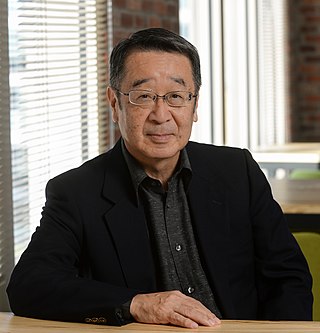
Yoshihisa Yamamoto is the director of Physics & Informatics Laboratories, NTT Research, Inc. He is also Professor (Emeritus) at Stanford University and National Institute of Informatics (Tokyo).
A trion is a localized excitation which consists of three charged particles. A negative trion consists of two electrons and one hole and a positive trion consists of two holes and one electron. The trion itself is a quasiparticle and is somewhat similar to an exciton, which is a complex of one electron and one hole. The trion has a ground singlet state (spin S = 1/2) and an excited triplet state (S = 3/2). Here singlet and triplet degeneracies originate not from the whole system but from the two identical particles in it. The half-integer spin value distinguishes trions from excitons in many phenomena; for example, energy states of trions, but not excitons, are split in an applied magnetic field. Trion states were predicted theoretically in 1958; they were observed experimentally in 1993 in CdTe/Cd1−xZnxTe quantum wells, and later in various other optically excited semiconductor structures. There are experimental proofs of their existence in nanotubes supported by theoretical studies. Despite numerous reports of experimental trion observations in different semiconductor heterostructures, there are serious concerns on the exact physical nature of the detected complexes. The originally foreseen 'true' trion particle has a delocalized wavefunction (at least at the scales of several Bohr radii) while recent studies reveal significant binding from charged impurities in real semiconductor quantum wells.
Electrically detected magnetic resonance (EDMR) is a materials characterisation technique that improves upon electron spin resonance. It involves measuring the change in electrical resistance of a sample when exposed to certain microwave frequencies. It can be used to identify very small numbers of impurities in semiconductors.
Bilayer graphene is a material consisting of two layers of graphene. One of the first reports of bilayer graphene was in the seminal 2004 Science paper by Geim and colleagues, in which they described devices "which contained just one, two, or three atomic layers"
Bose–Einstein condensation can occur in quasiparticles, particles that are effective descriptions of collective excitations in materials. Some have integer spins and can be expected to obey Bose–Einstein statistics like traditional particles. Conditions for condensation of various quasiparticles have been predicted and observed. The topic continues to be an active field of study.

Transition-metal dichalcogenide (TMD or TMDC) monolayers are atomically thin semiconductors of the type MX2, with M a transition-metal atom (Mo, W, etc.) and X a chalcogen atom (S, Se, or Te). One layer of M atoms is sandwiched between two layers of X atoms. They are part of the large family of so-called 2D materials, named so to emphasize their extraordinary thinness. For example, a MoS2 monolayer is only 6.5 Å thick. The key feature of these materials is the interaction of large atoms in the 2D structure as compared with first-row transition-metal dichalcogenides, e.g., WTe2 exhibits anomalous giant magnetoresistance and superconductivity.
A two-dimensional semiconductor is a type of natural semiconductor with thicknesses on the atomic scale. Geim and Novoselov et al. initiated the field in 2004 when they reported a new semiconducting material graphene, a flat monolayer of carbon atoms arranged in a 2D honeycomb lattice. A 2D monolayer semiconductor is significant because it exhibits stronger piezoelectric coupling than traditionally employed bulk forms. This coupling could enable applications. One research focus is on designing nanoelectronic components by the use of graphene as electrical conductor, hexagonal boron nitride as electrical insulator, and a transition metal dichalcogenide as semiconductor.
Integrated quantum photonics, uses photonic integrated circuits to control photonic quantum states for applications in quantum technologies. As such, integrated quantum photonics provides a promising approach to the miniaturisation and scaling up of optical quantum circuits. The major application of integrated quantum photonics is Quantum technology:, for example quantum computing, quantum communication, quantum simulation, quantum walks and quantum metrology.
Graphene is a semimetal whose conduction and valence bands meet at the Dirac points, which are six locations in momentum space, the vertices of its hexagonal Brillouin zone, divided into two non-equivalent sets of three points. The two sets are labeled K and K'. The sets give graphene a valley degeneracy of gv = 2. By contrast, for traditional semiconductors the primary point of interest is generally Γ, where momentum is zero. Four electronic properties separate it from other condensed matter systems.
Spin squeezing is a quantum process that decreases the variance of one of the angular momentum components in an ensemble of particles with a spin. The quantum states obtained are called spin squeezed states. Such states can be used for quantum metrology, as they can provide a better precision for estimating a rotation angle than classical interferometers.
References
- ↑ Behnia, Kamran (2012-07-01). "Polarized light boosts valleytronics". Nature Nanotechnology. 7 (8): 488–489. Bibcode:2012NatNa...7..488B. doi:10.1038/nnano.2012.117. ISSN 1748-3387. PMID 22751224.
- ↑ Nebel, Christoph E. (2013). "Electrons dance in diamond". Nature Materials. 12 (8): 690–691. Bibcode:2013NatMa..12..690N. doi:10.1038/nmat3724. ISSN 1476-1122. PMID 23877395.
- ↑ Gunawan, O.; Habib, B.; De Poortere, E. P.; Shayegan, M. (2006-10-30). "Quantized conductance in an AlAs two-dimensional electron system quantum point contact". Physical Review B. 74 (15): 155436. arXiv: cond-mat/0606272 . Bibcode:2006PhRvB..74o5436G. doi:10.1103/PhysRevB.74.155436. S2CID 119086726.
- 1 2 Culcer, Dimitrie; et al. (2012). "Valley-Based Noise-Resistant Quantum Computation Using Si Quantum Dots". Physical Review Letters. 108 (12): 126804. arXiv: 1107.0003 . Bibcode:2012PhRvL.108l6804C. doi:10.1103/PhysRevLett.108.126804. PMID 22540611. S2CID 22859674.
- ↑ "Universal quantum computing with spin and valley states". Niklas Rohling and Guido Burkard. New J. Phys.14, 083008(2012).
- 1 2 "A valley–spin qubit in a carbon nanotube". E. A. Laird, F. Pei & L. P. Kouwenhoven. Nature Nanotechnology8, 565–568 (2013).
- ↑ Prati, Enrico (2011-10-01). "Valley Blockade Quantum Switching in Silicon Nanostructures". Journal of Nanoscience and Nanotechnology. 11 (10): 8522–8526. arXiv: 1203.5368 . doi:10.1166/jnn.2011.4957. ISSN 1533-4880. PMID 22400218. S2CID 28847674.
- ↑ Crippa A; et al. (2015). "Valley blockade and multielectron spin-valley Kondo effect in silicon". Physical Review B. 92 (3): 035424. arXiv: 1501.02665 . Bibcode:2015PhRvB..92c5424C. doi:10.1103/PhysRevB.92.035424. S2CID 117310207.
- ↑ A. Rycerz; et al. (2007). "Valley filter and valley valve in graphene". Nature Physics. 3 (3): 172–175. arXiv: cond-mat/0608533 . Bibcode:2007NatPh...3..172R. doi:10.1038/nphys547. S2CID 119377206.
- ↑ Mrudul, M.S.; Galan, A.J.; Ivanov, M.; Dixit, G. (2021). "Light-induced valleytronics in pristine graphene". Optica. 8 (3): 422–427. arXiv: 2011.04973 . Bibcode:2021Optic...8..422M. doi:10.1364/OPTICA.418152.
- ↑ Rana, N.; Dixit, G. (2023). "All-optical ultrafast valley switching in two-dimensional materials". Physical Review Applied. 19 (3): 034056. Bibcode:2023PhRvP..19c4056R. doi:10.1103/PhysRevApplied.19.034056.
- ↑ Ang, Y.S.; Yang, S.A.; Zhang, C.; Ma, Z.S.; Ang, L.K. (2017). "Valleytronics in merging Dirac cones: All-electric-controlled valley filter, valve, and universal reversible logic gate". Physical Review B. 96 (24): 245410. arXiv: 1711.05906 . Bibcode:2017PhRvB..96x5410A. doi:10.1103/PhysRevB.96.245410. S2CID 51933139.
- ↑ "Valley polarization in MoS2 monolayers by optical pumping". Hualing Zeng, Junfeng Dai, Wang Yao, Di Xiao and Xiaodong Cui. Nature Nanotechnology7, 490–493 (2012).
- ↑ Wu, Zefei; Zhou, Benjamin T.; Cai, Xiangbin; Cheung, Patrick; Liu, Gui-Bin; Huang, Meizhen; Lin, Jiangxiazi; Han, Tianyi; An, Liheng; Wang, Yuanwei; Xu, Shuigang; Long, Gen; Cheng, Chun; Law, Kam Tuen; Zhang, Fan (2019-02-05). "Intrinsic valley Hall transport in atomically thin MoS2". Nature Communications. 10 (1): 611. doi:10.1038/s41467-019-08629-9. ISSN 2041-1723. PMC 6363770 . PMID 30723283.
- ↑ Bussolotti, Fabio; Kawai, Hiroyo; Ooi, Zi En; Chellappan, Vijila; Thian, Dickson; Pang, Ai Lin Christina; Goh, Kuan Eng Johnson (2018). "Roadmap on finding chiral valleys: screening 2D materials for valleytronics". Nano Futures. 2 (3): 032001. Bibcode:2018NanoF...2c2001B. doi:10.1088/2399-1984/aac9d7. S2CID 139826293.
- ↑ "Generation, transport and detection of valley-polarized electrons in diamond". Jan Isberg, Markus Gabrysch, Johan Hammersberg, Saman Majdi, Kiran Kumar Kovi and Daniel J. Twitchen. Nature Materials12, 760–764 (2013). doi:10.1038/nmat3694
- ↑ "Field-induced polarization of Dirac valleys in bismuth". Zengwei Zhu, Aurélie Collaudin, Benoît Fauqué, Woun Kang and Kamran Behnia. Nature Physics8, 89-94 (2011).
- ↑ Takashina, K. (2006). "Valley Polarization in Si(100) at Zero Magnetic Field". Physical Review Letters. 96 (23): 236801. arXiv: cond-mat/0604118 . Bibcode:2006PhRvL..96w6801T. doi:10.1103/PhysRevLett.96.236801. PMID 16803388. S2CID 42747323.
- ↑ Yang, C. H.; Rossi, A.; Ruskov, R.; Lai, N. S.; Mohiyaddin, F. A.; Lee, S.; Tahan, C.; Klimeck, G.; Morello, A. (2013-06-27). "Spin-valley lifetimes in a silicon quantum dot with tunable valley splitting". Nature Communications. 4: 2069. arXiv: 1302.0983 . Bibcode:2013NatCo...4.2069Y. doi:10.1038/ncomms3069. ISSN 2041-1723. PMID 23804134. S2CID 13978092.
- ↑ "AlAs two-dimensional electrons in an antidot lattice: Electron pinball with elliptical Fermi contours". O. Gunawan, E. P. De Poortere, and M. Shayegan. Phys. Rev. B75, 081304(R)(2007).
- ↑ "Spin valleytronics in silicene: Quantum spin Hall–quantum anomalous Hall insulators and single-valley semimetals". Motohiko Ezawa, Phys. Rev. B87, 155415 (2013)