COP400

Last updated
National Semiconductor COP400
NationalSemiCOP420-JLA-N.jpg
National Semiconductor COP420 in 28-pin plastic DIP. Late 1982 date code.
General information
Launched1977;47 years ago (1977)
Common manufacturer(s)
Performance
Max. CPU clock rate to 250 KHz
Data width4 (RAM), 8 (ROM)
Address width7 (RAM), 11 (ROM)
Architecture and classification
ApplicationEmbedded
Instruction set COP400
Number of instructions40
Physical specifications
Package(s)
  • 24, 28, 40-pin DIP
History
Predecessor(s)MM5799 (PMOS COP)
Successor(s) COP8

The COP400 or COP II is a 4-bit microcontroller family introduced in 1977 by National Semiconductor as a follow-on product to their original PMOS COP microcontroller. [1] COP400 family members are complete microcomputers containing internal timing, logic, ROM, RAM, and I/O necessary to implement dedicated controllers. [2] Some COP400 devices were second-sourced by Western Digital as the WD4200 family. [3] [4] In the Soviet Union several COP400 microcontrollers were manufactured as the 1820 series (e.g. the COP402 with designation КР1820ВЕ1). [5]

Contents

The COP400 is implemented in CMOS or N-channel silicon gate MOS technology. It was typically packaged in 24- or 28-pin DIP packages. Instruction cycle time of the faster family members is 4 microseconds. The COP400 family offered several memory and pinout configurations.

Notable products that used COP400-family chips include the Apple Lisa, Milton Bradley and Mattel electronic games, Coleco Head to Head Basketball, the Grundy Newbrain, and others.

Memory

The COP400 uses separate memory spaces for ROM and RAM. ROM addresses are 11-bit maximum, while data addresses are 7-bit maximum.

National Semiconductor COP410L die image National Semiconductor COP410L NGS top metal.jpg
National Semiconductor COP410L die image

ROM

Program memory consists of a 512, 1024, or 2048 × 8-bit ROM. ROM bytes may be program instructions, program data, or jump address pointers. Due to the special characteristics associated with the JP and JSRP instructions, ROM must often be conceived of as organized into pages of 64 bytes each. Also, because of the unique operations performed by the LQID and JID instructions, ROM pages must sometimes be thought of as organized into blocks of 256 bytes.

RAM

Data memory consists of a 32, 64, or 128 × 4-bit RAM, organized as several data registers of 16 4-bit digits. RAM addressing is implemented by the 6- or 7-bit B register used as a pointer. The B register's upper 2 or 3 bits (Br) select one of 4 or 8 data registers and lower 4 bits (Bd) select one of 16 4-bit digits in the selected data register. The 4-bit contents of the RAM digit pointed to by the B register are usually loaded into, exchanged with, or operate on the A register.

CPU registers

COP400 registers
1009080706050403020100(bit position)
 AAccumulator
 BrBdB (pointer)
PC (high)PC (page)Program Counter
SAStack Registers
SB
SC
Status flag
  C Carry Flag

The register configuration shown in the diagram is for the COP400 family members with maximum ROM (2048 × 8 bits) and RAM (128 × 4 bits). Family members with only 512 or 1024 bytes of ROM will have only a 9- or 10-bit PC. Those with 64 or 32 locations of RAM will have only a 2-bit Br register. Some low end family members omit the SC stack register. [6]

The 4-bit A register (accumulator) is the source and destination register for most arithmetic, logic, and data memory access operations. It can also be used to load the Br and Bd portions of the B register, to load and input 4 bits of the 8-bit Q latch data, to input 4 bits of the 8-bit L port and to perform data exchanges with the SIO register.

A 4-bit ALU performs the arithmetic and logic functions, storing results in A. ASC and CASC operations output a carry to the 1-bit C register, most often employed to indicate arithmetic overflow.

All ROM addressing is accomplished via the 9-, 10-, or 11-bit PC register. Its binary value selects one of the bytes contained in ROM, usually the next program instruction. The value of PC is automatically incremented by 1 prior to the execution of the current instruction to point to the next sequential ROM location, unless the current instruction is a transfer of control instruction. In the latter case, PC is loaded with the appropriate non-sequential value to implement the transfer of control operation. The PC automatically rolls over to point to the next 64 byte page or 256 byte block of program memory. The upper 1, 2, or 3 bits of PC are also used in the JID and LQID instructions.

Three levels of subroutine are implemented by the subroutine save registers, SA, SB, and SC, providing a last-in, first-out (LIFO) hardware subroutine stack. Some implementations do not have a SC.

I/O registers and ports

There are no port numbers or memory addresses associated with the COP400 I/O devices. All the physical I/O registers and ports are referenced by the COP400 assembly language directly by name.

Baseline

Nearly all COP400 family devices implement the following: [6]

High end

There are a few high end members of the COP400 family such as the COP440 and COP2440 that have 40-pins. These have additional registers and ports: [7]

Instruction set

The COP400 family is designed to have very compact code. The most frequently used instructions are one byte. In some cases there are special one-byte forms of two byte instructions. Some features that can be used to make object code more compact are:

COP400 family instruction set
OpcodeOperandMnemonicDescriptionSkip
76543210
00000000CLRAA ← 0
000b000b11SKMBZ bRAM(B)b = 0
00000010XORA ← A RAM(B)
00r0100XIS rA ↔ RAM(B), Br ← Br r, Bd ← Bd + 1Bd = 0
00r0101LD rA ← RAM(B), Br ← Br r
00r0110X rA ↔ RAM(B), Br ← Br r
00r0111XDS rA ↔ RAM(B), Br ← Br r, Bd ← Bd - 1Bd = 15
00r1dLBI r,dBr ← r, Bd ← (d + 9) ^ 15 (Br = 0-3, Bd = 9-15, 0)next LBI
00010000CASCA ← ~A + RAM(B) + C, C ← Carrycarry
00010010XABRA ↔ Br, A3 ← 0
00100000SKCC = 1
00100001SKEA = RAM(B)
00100010SCC ← 1
001000110rrrddddLDD r,dA ← RAM(r,d)
001000111rrrddddXAD r,dA ↔ RAM(r,d)
00110000ASCA ← A + RAM(B) + C, C ← Carrycarry
00110001ADDA ← A + RAM(B)
00110010RCC ← 0
00110011opcode33H prefixSee table below for instructions with this prefix
01000000COMPA ← ~A
01000001SKTSkip on timer overflowtimer
01000010RMB 2RAM(B)2 ← 0
01000011RMB 3RAM(B)3 ← 0
01000100NOPNo operation
01000101RMB 1RAM(B)1 ← 0
01000110SMB 2RAM(B)2 ← 1
01000111SMB 1RAM(B)1 ← 1
01001000RETPop PC (PC ← SA, SA ← SB, SB ← SC)
01001001RETSKPop PCalways
01001010ADTA ← A + 10
01001011SMB 3RAM(B)3 ← 1
01001100RMB 0RAM(B)0 ← 0
01001101SMB 0RAM(B)0 ← 1
01001110CBAA ← Bd
01001111XASA ↔ SIO, SK ← C
01010000CABBd ← A
0101yAISC yA ← A + y (1 ≤ y ≤ 15)carry
01100addhiaddloJMP aPC[10:8] ← addhi, PC[7:0] ← addlo
01101addhiaddloJSR aPush PC, PC[10:8] ← addhi, PC[7:0] ← addlo
0111ySTII yRAM(B) ← y, Bd ← Bd + 1
10addrJSRP aIf PC[10:6] ≠ 00010: Push PC, PC[10:6] ← 00010, PC[5:0] ← addr
10111111LQIDQ ← ROM(PC[10:8], A, RAM(B)), SC ← SB
11addrJP aIf PC[10:6] ≠ 00010: PC[5:0] ← addr
1addrJP aIf PC[10:7] = 0001: PC[6:0] ← addr
11111111JIDPC[7:0] ← ROM(PC[10:8], A, RAM(B))
76543210OperandMnemonicDescriptionSkip
opcodes prefixed with 33H
OpcodeMnemonicDescriptionSkipNon-core Instruction
76543210
000b000b11SKGBZ bGb = 0
00001011XANA[1:0] ↔ N, A[2:3] ← 0Y
00001111CEMARAM(B) ← EN[7:4], A ← EN[3:0]Y
00011001LIDRAM(B), A ← ROM(PC[10:8], A, RAM(B))Y
00011111CAMEEN[7:4] ← A, EN[3:0] ← RAM(B)Y
00100001SKGZG = 0
00101000ININA ← IN
00101001INILA ← IL3, 1, 0, IL0 or A ← IL3, CKO, 0, IL0
00101010INGA ← G
00101011INHA ← HY
00101100CQMARAM(B) ← Q[7:4], A ← Q[3:0]
00101101INRRAM(B) ← R[7:4], A ← R[3:0]Y
00101110INLRAM(B) ← L[7:4], A ← L[3:0]
00101111CTMARAM(B) ← T[7:4], A ← T[3:0]Y
00111010OMGG ← RAM(B)
00111011OMHH ← RAM(B)Y
00111100CAMQQ[7:4] ← A, Q[3:0] ← RAM(B)
00111101CAMRR[7:4] ← A, R[3:0] ← RAM(B)Y
00111110OBDD ← Bd
00111111CAMTT[7:4] ← A, T[3:0] ← RAM(B)Y
0101yOGI yG ← y
0110yLEI yEN ← y
1rdLBI r,dBr ← r, Bd ← dnext LBI
76543210MnemonicDescriptionSkipNon-core

Example code

This example code demonstrates several of the space saving features on the instruction set:

            040 09      041 19      042 2F       043 15      044 14      045 C3      046 48 
; Copy a block of memory from one location to another.;; There are three entry points: copyA, copyB, and copyC.; The values of the LBI instructions are expressed as; LBI Br, Bd.;copyA:LBI0,10;Copy 6 nybbles starting 0,10 to 1,10copyB:LBI1,10;Copy 6 nybbles starting 1,10 to 0,10copyC:LBI2,0;Copy 16 nybbles starting 2,0 to 3,0loop:LD1;Load src in A. XOR Br with 1 to get destXIS1;Save A in dest. Inc Bd. XOR Br with 1 to get srcJPloop;loop until Bd goes past last digit locationRET

Interrupt

Early COP400 devices that have 28 pins or more support a single interrupt. The IN 1 line is used as the interrupt input. Interrupt is enabled by setting bit 1 of the EN register to 1 with a LEI instruction. In response to low-going pulse of at least two instruction cycles long on IN 1, all transfer of control instructions such as JP are completed and all sequential LBI instructions are executed. The PC is then pushed on the subroutine stack and control is transferred to the interrupt handler at address 0xFF. No subroutines may be called in the interrupt service routine on devices with a hardware stack. [6] Curiously, later devices such as the COP440 support four interrupt sources and two service routines but only one interrupt source can be selected at a time. Subroutines are supported inside interrupt service routines on devices with a stack pointer.

Architectural extensions

Although the majority of COP400 devices were targeted at low-end applications, several extensions to the architecture were created to address more demanding applications. Dual CPU, a deeper stack in RAM, and larger address spaces were added to some devices by 1985. [7]

Dual CPU

“Dual CPU” versions of the COP400 were announced by National Semiconductor in 1981. These single-chip barrel processors contain two ostensibly independent CPUs that share instructions, memory, and most IO devices. In reality, the CPUs are not fully independent and share hardware resources similar to Intel processors with Hyper-Threading Technology (HTT). Like HTT, the dual CPU version works by duplicating certain sections of the processor—those that store the architectural state—but not duplicating the main execution resources such as ALU, buses, and memory. Separate architectural states for each of the two virtual processors is established with duplicated A (accumulators), B (pointer registers), C (carry flags), N (stack pointers), and PC (program counters). [6]

When the reset is deasserted, both processors start at location 0 which contains a CLRA instruction, then one processor jumps to location 401 (hex) followed an instruction cycle later by the second processor executing location 1. The processors will then alternately execute one byte of code each.

At maximum clock frequency, the instruction execution time (single byte instruction) for each processor is 4 microseconds, hence, the instruction cycle time for either processor is twice that amount, 8 microseconds.

Some dual CPU versions include the 40-pin COP2440N, the 28-pin COP2441N, and the 24-pin COP2442N.

Return stack in RAM

COP400 with stack pointer
1009080706050403020100(bit position)
 AAccumulator
 BrBdB (pointer)
 1 0 0 0N0 0Stack Pointer
PC (high)PC (page)Program Counter
Status flag
  C Carry Flag
(COP440 shown)

Earlier COP400 devices included a two or three level dedicated hardware return stack. Later devices such as the COP440 feature a 4-level return stack implemented with a 2-bit stack pointer and RAM. Dual CPU versions have two separate 4-level return stacks implemented with a two 2-bit stack pointers and two different RAM areas.

Larger address space

The basic COP400 instruction set supports ROM addresses of up to 11-bits (2,048 bytes), while data addresses are 7-bits maximum (128 locations). The so-called group 4 devices extended the memory limit by adding three-byte JMP, JSR, and LBI instructions with more address bits. These support ROM addresses of 15-bits maximum (32,768 bytes), while data addresses are 9-bits maximum (512 locations). Devices that support these instructions include COP408, COP484, COP485, C0P409. It is unclear whether any of these group 4 devices were produced.

Applications

Emulator

There is an open-source MAME emulator for the COP400 family and several hand held games and specialty calculators. [12] [13]

See also

Related Research Articles

<span class="mw-page-title-main">Intel 8080</span> 8-bit microprocessor

The Intel 8080 ("eighty-eighty") is the second 8-bit microprocessor designed and manufactured by Intel. It first appeared in April 1974 and is an extended and enhanced variant of the earlier 8008 design, although without binary compatibility. The initial specified clock rate or frequency limit was 2 MHz, with common instructions using 4, 5, 7, 10, or 11 cycles. As a result, the processor is able to execute several hundred thousand instructions per second. Two faster variants, the 8080A-1 and 8080A-2, became available later with clock frequency limits of 3.125 MHz and 2.63 MHz respectively. The 8080 needs two support chips to function in most applications: the i8224 clock generator/driver and the i8228 bus controller. It is implemented in N-type metal–oxide–semiconductor logic (NMOS) using non-saturated enhancement mode transistors as loads thus demanding a +12 V and a −5 V voltage in addition to the main transistor–transistor logic (TTL) compatible +5 V.

<span class="mw-page-title-main">Motorola 68000</span> Microprocessor

The Motorola 68000 is a 16/32-bit complex instruction set computer (CISC) microprocessor, introduced in 1979 by Motorola Semiconductor Products Sector.

<span class="mw-page-title-main">Zilog Z80</span> 8-bit microprocessor

The Z80 is an 8-bit microprocessor introduced by Zilog as the startup company's first product. The Z80 was conceived by Federico Faggin in late 1974 and developed by him and his 11 employees starting in early 1975. The first working samples were delivered in March 1976, and it was officially introduced on the market in July 1976. With the revenue from the Z80, the company built its own chip factories and grew to over a thousand employees over the following two years.

<span class="mw-page-title-main">MCS-51</span> Single chip microcontroller series by Intel

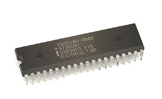
The Intel MCS-51 is a single chip microcontroller (MCU) series developed by Intel in 1980 for use in embedded systems. The architect of the Intel MCS-51 instruction set was John H. Wharton. Intel's original versions were popular in the 1980s and early 1990s, and enhanced binary compatible derivatives remain popular today. It is a complex instruction set computer, but also has some of the features of RISC architectures, such as a large register set and register windows, and has separate memory spaces for program instructions and data.

<span class="mw-page-title-main">Intel 8085</span> 8-bit microprocessor by Intel

The Intel 8085 ("eighty-eighty-five") is an 8-bit microprocessor produced by Intel and introduced in March 1976. It is the last 8-bit microprocessor developed by Intel.

<span class="mw-page-title-main">Intel 4040</span> 4-bit microprocessor introduced in 1974 by Intel

The Intel 4040 microprocessor was the successor to the Intel 4004, introduced in 1974. The 4040 employed a 10 μm silicon gate enhancement-load PMOS technology, was made up of 3,000 transistors and could execute approximately 62,000 instructions per second.

<span class="mw-page-title-main">PIC microcontrollers</span> Line of single-chip microprocessors from Microchip Technology

PIC is a family of microcontrollers made by Microchip Technology, derived from the PIC1650 originally developed by General Instrument's Microelectronics Division. The name PIC initially referred to Peripheral Interface Controller, and is currently expanded as Programmable Intelligent Computer. The first parts of the family were available in 1976; by 2013 the company had shipped more than twelve billion individual parts, used in a wide variety of embedded systems.

<span class="mw-page-title-main">TI MSP430</span>

The MSP430 is a mixed-signal microcontroller family from Texas Instruments, first introduced on 14 February 1992. Built around a 16-bit CPU, the MSP430 was designed for low power consumption embedded applications and low cost.

The National Semiconductor COP8 is an 8-bit CISC core microcontroller. COP8 is an enhancement to the earlier COP400 4-bit microcontroller family. COP8 main features are:

The TMS9900 was one of the first commercially available, single-chip 16-bit microprocessors. Introduced in June 1976, it implemented Texas Instruments' TI-990 minicomputer architecture in a single-chip format, and was initially used for low-end models of that lineup.

<span class="mw-page-title-main">Fairchild F8</span> 8-bit microprocessor first shipped in 1975

The Fairchild F8 is an 8-bit microprocessor system from Fairchild Semiconductor, announced in 1974 and shipped in 1975. The original processor family included four main 40-pin integrated circuits (ICs); the 3850 CPU which was the arithmetic logic unit, the 3851 Program Storage Unit (PSU) which contained 1 KB of program ROM and handled instruction decoding, and the optional 3852 Dynamic Memory Interface (DMI) or 3853 Static Memory Interface (SMI) to control additional RAM or ROM holding the user programs or data. The 3854 DMA was another optional system that added direct memory access into the RAM controlled by the 3852.

<span class="mw-page-title-main">National Semiconductor SC/MP</span> 8-bit microprocessor

National Semiconductor's SC/MP for Simple Cost-effective Micro Processor, is an early 8-bit microprocessor which became available in April 1976. It was designed to allow systems to be implemented with the minimum number of additional support chips. SC/MP included a daisy-chained control pin that allowed up to three SC/MP's share a single main memory to produce a multiprocessor system, or to act as controllers in a system with another main central processing unit (CPU). Three versions were released over its lifetime, SCMP-1 through 3, the latter two also known as INS8060 and INS8070.

The Atmel AVR instruction set is the machine language for the Atmel AVR, a modified Harvard architecture 8-bit RISC single chip microcontroller which was developed by Atmel in 1996. The AVR was one of the first microcontroller families to use on-chip flash memory for program storage.

<span class="mw-page-title-main">Signetics 2650</span> 8-bit microprocessor

The Signetics 2650 was an 8-bit microprocessor introduced in July 1975. According to Adam Osborne's book An Introduction to Microprocessors Vol 2: Some Real Products, it was "the most minicomputer-like" of the microprocessors available at the time. A combination of missing features and odd memory access limited its appeal, and the system saw little use in the market.

TLCS is a prefix applied to microcontrollers made by Toshiba. The product line includes multiple families of CISC and RISC architectures. Individual components generally have a part number beginning with "TMP". E.g. the TMP8048AP is a member of the TLCS-48 family.

<span class="mw-page-title-main">Intersil 6100</span> 12-bit microprocessor

The Intersil 6100 is a single-chip microprocessor implementation of the 12-bit PDP-8 instruction set, along with a range of peripheral support and memory ICs developed by Intersil in the mid-1970s. It was sometimes referred to as the CMOS-PDP8. Since it was also produced by Harris Corporation, it was also known as the Harris HM-6100. The Intersil 6100 was introduced in the second quarter of 1975, and the Harris version in 1976.

The 9S08 is an 8-bit microcontroller (µC) family originally produced by Motorola, later by Freescale Semiconductor, and currently by NXP, descended from the Motorola 6800 microprocessor. It is a CISC microcontroller. A slightly extended variant of the 68HC08, it shares upward compatibility with the aging 68HC05 microcontrollers, and is found in almost any type of embedded systems. The larger members offer up to 128 KiB of flash, and 8 KiB of RAM via a simple memory management unit (MMU) which allows bank-switching 16 KiB of the address space and an address/data register pair which allows data fetches from any address. The paging scheme used allows for a theoretical maximum of 4 MB of flash.

<span class="mw-page-title-main">ST6 and ST7</span> 8-bit microcontroller product lines from STMicroelectronics

The ST6 and ST7 are 8-bit microcontroller product lines from STMicroelectronics. They are commonly used in small embedded applications like washing machines.

<span class="mw-page-title-main">STM8</span>

The STM8 is an 8-bit microcontroller family by STMicroelectronics. The STM8 microcontrollers use an extended variant of the ST7 microcontroller architecture. STM8 microcontrollers are particularly low cost for a full-featured 8-bit microcontroller.

The Mostek MK5065 was an 8-bit microprocessor introduced by Mostek in early 1974. The design was originally developed by Motorola for use in an Olivetti electronic calculator, and was licensed to Mostek for use in non-calculator roles. It featured three sets of processor registers, allowing it to switch to an interrupt handler in a single cycle, and a wait-for-data mode that aided direct memory access.

References

  1. "National Semiconductor: The COP before the COPS". The CPUSHACK Museum. 27 September 2014. Retrieved 23 December 2021.
  2. "COP400 Microcontroller Family COPS Family User's Guide". National Semiconductor. Retrieved 3 August 2023.
  3. "Western Digital and the COP". The CPUSHACK Museum. 2 October 2015. Retrieved 22 December 2021.
  4. "WD4200/WD4210 Single-Chip N-Channel Microcontroilers" . Retrieved 23 December 2021.
  5. "Soviet microprocessors, microcontrollers, FPU chips and their western analogs". www.cpu-world.com. Retrieved 15 November 2022.
  6. 1 2 3 4 "COPS Microcontrollers Data Book". National Semiconductor. Retrieved 19 January 2022.
  7. 1 2 "The COPS Programming Manual (1985)" (PDF). Vintage Technology Digital Archive. National Semiconductor. Retrieved 23 December 2021.
  8. "Apple Lisa 341-0064A (COP421)". Visual6502. Retrieved 24 December 2021.
  9. "National Semiconductor COP400". Sean Riddle. Retrieved 24 December 2021.
  10. "1983 Components Catalog" (PDF). Western Digital. p. 621. Retrieved 24 December 2021.
  11. "COP420 4-Bit Processor - Newbrain" . Retrieved 30 December 2021.
  12. "COP400 libmame repository". Github. Retrieved 23 April 2022.
  13. "Funjacks (example emulated game)". Arcade Database. Retrieved 23 April 2022.