Carrier lifetime

Last updated

A definition in semiconductor physics, carrier lifetime is defined as the average time it takes for a minority carrier to recombine. The process through which this is done is typically known as minority carrier recombination.

Contents

The energy released due to recombination can be either thermal, thereby heating up the semiconductor (thermal recombination or non-radiative recombination, one of the sources of waste heat in semiconductors), or released as photons (optical recombination, used in LEDs and semiconductor lasers). The carrier lifetime can vary significantly depending on the materials and construction of the semiconductor.

Carrier lifetime plays an important role in bipolar transistors and solar cells.

In indirect band gap semiconductors, the carrier lifetime strongly depends on the concentration of recombination centers. Gold atoms act as highly efficient recombination centers, silicon for some high switching speed diodes and transistors is therefore alloyed with a small amount of gold. Many other atoms, e.g. iron or nickel, have similar effect. [1]

Overview

In practical applications, the electronic band structure of a semiconductor is typically found in a non-equilibrium state. Therefore, processes that tend towards thermal equilibrium, namely mechanisms of carrier recombination, always play a role.

Additionally, semiconductors used in devices are very rarely pure semiconductors. Oftentimes, a dopant is used, giving an excess of electrons (in so-called n-type doping) or holes (in so-called p-type doping) within the band structure. This introduces a majority carrier and a minority carrier. As a result of this, the carrier lifetime plays a vital role in many semiconductor devices that have dopants.

Recombination mechanisms

There are several mechanisms by which minority carriers can recombine, each of which subtract from the carrier lifetime. The main mechanisms that play a role in modern devices are band-to-band recombination and stimulated emission, which are forms of radiative recombination, and Shockley-Read-Hall (SRH), Auger, Langevin, and surface recombination, which are forms of non-radiative recombination.

Depending on the system, certain mechanisms may play a greater role than others. [2] For example, surface recombination plays a significant role in solar cells, where much of the effort goes into passivating surfaces to minimize non-radiative recombination. [3] As opposed to this, Langevin recombination plays a major role in organic solar cells, where the semiconductors are characterized by low mobility. [4] In these systems, maximizing the carrier lifetime is synonymous to maximizing the efficiency of the device. [5]

Applications

Solar cells

A solar cell is an electrical device in which a semiconductor is exposed to light that is converted into electricity through the photovoltaic effect. Electrons are either excited through the absorption of light, or if the band-gap energy of the material can be bridged, electron-hole pairs are created. Simultaneously, a voltage potential is created. The charge carriers within the solar cell move through the semiconductor in order to cancel said potential, which is the drifting force that moves the electrons. Also, the electrons can be forced to move by diffusion from higher concentration to lower concentration of electrons.

In order to maximize the efficiency of the solar cell, it is desirable to have as many charge carriers as possible collected at the electrodes of the solar cell. Thus, recombination of electrons (among other factors that influence efficiency) must be avoided. This corresponds to an increase in the carrier lifetime. Surface recombination occurs at the top of the solar cell, which makes it preferable to have layers of material that have great surface passivation properties so as not to become affected by exposure to light over longer periods of time. [6] Additionally, the same method of layering different semiconductor materials is used to reduce the capture probability of the electrons, which results in a decrease in trap-assisted SRH recombination, and an increase in carrier lifetime. Radiative (band-to-band) recombination is negligible in solar cells that have semiconductor materials with indirect bandgap structure. Auger recombination occurs as a limiting factor for solar cells when the concentration of excess electrons grows large at low doping rates. Otherwise, the doping-dependent SRH recombination is one of the primary mechanisms that reduces the electrons’ carrier lifetime in solar cells. [7]

Bipolar junction transistors

A bipolar junction transistor is a type of transistor that is able to use electrons and electron holes as charge carriers. A BJT uses a single crystal of material in its circuit that is divided into two types of semiconductor, an n-type and p-type. These two types of doped semiconductors are spread over three different regions in respective order: the emitter region, the base region and the collector region. The emitter region and collector region are quantitively doped differently, but are of the same type of doping and share a base region, which is why the system is different from two diodes connected in series with each other. For a PNP-transistor, these regions are, respectively, p-type, n-type and p-type, and for a NPN-transistor, these regions are, respectively, n-type, p-type and n-type.

For NPN-transistors in typical forward-active operation, given an injection of charge carriers through the first junction from the emitter into the base region, electrons are the charge carriers that are transported diffusively through the base region towards the collector region. These are the minority carriers of the base region. Analogously, for PNP-transistors, electronic holes are the minority carriers of the base region.

The carrier lifetime of these minority carriers plays a crucial role in the charge flow of minority carriers in the base region, which is found between the two junctions. Depending on the BJT's mode of operation, recombination is either preferred, or to be avoided in the base region.

In particular, for the aforementioned forward-active mode of operation, recombination is not preferable. Thus, in order to get as many minority carriers as possible from the base region into the collecting region before these recombine, the width of the base region must be small enough such that the minority carriers can diffuse in a smaller amount of time than the semiconductor's minority carrier lifetime. Equivalently, the width of the base region must be smaller than the diffusion length, which is the average length a charge carrier travels before recombining. Additionally, in order to prevent high rates of recombination, the base is only lightly doped with respect to the emitter and collector region. As a result of this, the charge carriers do not have a high probability of staying in the base region, which is their preferable region of occupation when recombining into a lower-energy state.

For other modes of operation, like that of fast switching, a high recombination rate (and thus a short carrier lifetime) is desirable. The desired mode of operation, and the associated properties of the doped base region must be considered in order to facilitate the appropriate carrier lifetime. Presently, silicon and silicon carbide are the materials used in most BJTs. [8] The recombination mechanisms that must be considered in the base region are surface recombination near the base-emitter junction, as well as SRH- and Auger recombination in the base region. Specifically, Auger recombination increases when the amount of injected charge carriers grows, hence decreasing the efficiency of the current gain with growing injection numbers.

Semiconductor lasers

In semiconductor lasers, the carrier lifetime is the time it takes an electron before recombining via non-radiative processes in the laser cavity. In the frame of the rate equations model, carrier lifetime is used in the charge conservation equation as the time constant of the exponential decay of carriers.

The dependence of carrier lifetime on the carrier density is expressed as: [9]

where A, B and C are the non-radiative, radiative and Auger recombination coefficients and is the carrier lifetime.

Measurement

Because the efficiency of a semiconductor device generally depends on its carrier lifetime, it is important to be able to measure this quantity. The method by which this is done depends on the device, but is usually dependent on measuring the current and voltage.

In solar cells, the carrier lifetime can be calculated by illuminating the surface of the cell, which induces carrier generation and increases the voltage until it reaches an equilibrium, and subsequently turning off the light source. This causes the voltage to decay at a consistent rate. The rate at which the voltage decays is determined by the amount of minority carriers that recombine per unit time, with a higher amount of recombining carriers resulting in a faster decay. Subsequently, a lower carrier lifetime will result in a faster decay of the voltage. This means that the carrier lifetime of a solar cell can be calculated by studying its voltage decay rate. [10] This carrier lifetime is generally expressed as: [11]

where is the Boltzmann constant, q is the elementary charge, T is the temperature, and is the time derivative of the open-circuit voltage.

In bipolar junction transistors (BJTs), determining the carrier lifetime is rather more complicated. Namely, one must measure the output conductance and reverse transconductance, both of which are variables that depend on the voltage and flow of current through the BJT, and calculate the minority carrier transit time, which is determined by the width of the quasi-neutral base (QNB) of the BJT, and the diffusion coefficient; a constant that quantifies the atomic migration within the BJT. [12] This carrier lifetime is expressed as: [13]

where and are the output conductance, reverse transconductance, width of the QNB and diffusion coefficient, respectively.

Current research

Because a longer carrier lifetime is often synonymous to a more efficient device, research tends to focus on minimizing processes that contribute to the recombination of minority carriers. In practice, this generally implies reducing structural defects within the semiconductors, or introducing novel methods that do not suffer from the same recombination mechanisms.

In crystalline silicon solar cells, which are particularly common, an important limiting factor is the structural damage done to the cell when the transparent conducting film is applied. This is done with reactive plasma deposition, a form of sputter deposition. In the process of applying this film, defects appear on the silicon layer, which degrades the carrier lifetime. [14] Reducing the amount of damage done during this process is therefore important to increase the efficiency of the solar cell, and a focus of current research. [15]

In addition to research that seeks to optimize currently favoured technologies, there is a great deal of research surrounding other, less-utilized technologies, like the Perovskite solar cell (PSC). This solar cell is preferable due to its comparatively cheap and simple manufacturing process. Modern advancements suggest that there is still ample room to improve on the carrier lifetime of this solar cell, with most of the issues surrounding it being construction-related. [16]

In addition to solar cells, perovskites can be utilized to manufacture LEDs, lasers, and transistors. As a result of this, lead and halide perovskites are of particular interest in modern research. Current problems include the structural defects that appear when semiconductor devices are manufactured with the material, as the dislocation density associated with the crystals is a detriment to their carrier lifetime. [17]

Related Research Articles

<span class="mw-page-title-main">Diode</span> Two-terminal electronic component

A diode is a two-terminal electronic component that conducts current primarily in one direction. It has low resistance in one direction, and high resistance in the other.

<span class="mw-page-title-main">Semiconductor</span> Material that has electrical conductivity intermediate to that of a conductor and an insulator

A semiconductor is a material which has an electrical conductivity value falling between that of a conductor, such as copper, and an insulator, such as glass. Its resistivity falls as its temperature rises; metals behave in the opposite way. Its conducting properties may be altered in useful ways by introducing impurities ("doping") into the crystal structure. When two differently doped regions exist in the same crystal, a semiconductor junction is created. The behavior of charge carriers, which include electrons, ions, and electron holes, at these junctions is the basis of diodes, transistors, and most modern electronics. Some examples of semiconductors are silicon, germanium, gallium arsenide, and elements near the so-called "metalloid staircase" on the periodic table. After silicon, gallium arsenide is the second-most common semiconductor and is used in laser diodes, solar cells, microwave-frequency integrated circuits, and others. Silicon is a critical element for fabricating most electronic circuits.

<span class="mw-page-title-main">Semiconductor device</span> Electronic component that exploits the electronic properties of semiconductor materials

A semiconductor device is an electronic component that relies on the electronic properties of a semiconductor material for its function. Its conductivity lies between conductors and insulators. Semiconductor devices have replaced vacuum tubes in most applications. They conduct electric current in the solid state, rather than as free electrons across a vacuum or as free electrons and ions through an ionized gas.

<span class="mw-page-title-main">MOSFET</span> Type of field-effect transistor

The metal-oxide-semiconductor field-effect transistor is a type of field-effect transistor (FET), most commonly fabricated by the controlled oxidation of silicon. It has an insulated gate, the voltage of which determines the conductivity of the device. This ability to change conductivity with the amount of applied voltage can be used for amplifying or switching electronic signals. A metal-insulator-semiconductor field-effect transistor (MISFET) is a term almost synonymous with MOSFET. Another synonym is IGFET for insulated-gate field-effect transistor.

<span class="mw-page-title-main">Bipolar junction transistor</span> Transistor that uses both electrons and holes as charge carriers

A bipolar junction transistor (BJT) is a type of transistor that uses both electrons and electron holes as charge carriers. In contrast, a unipolar transistor, such as a field-effect transistor (FET), uses only one kind of charge carrier. A bipolar transistor allows a small current injected at one of its terminals to control a much larger current flowing between the terminals, making the device capable of amplification or switching.

<span class="mw-page-title-main">Schottky diode</span> Semiconductor diode

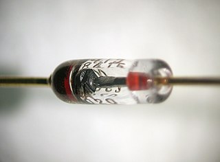
The Schottky diode, also known as Schottky barrier diode or hot-carrier diode, is a semiconductor diode formed by the junction of a semiconductor with a metal. It has a low forward voltage drop and a very fast switching action. The cat's-whisker detectors used in the early days of wireless and metal rectifiers used in early power applications can be considered primitive Schottky diodes.

In physics, a charge carrier is a particle or quasiparticle that is free to move, carrying an electric charge, especially the particles that carry electric charges in electrical conductors. Examples are electrons, ions and holes. The term is used most commonly in solid state physics. In a conducting medium, an electric field can exert force on these free particles, causing a net motion of the particles through the medium; this is what constitutes an electric current. In conducting media, particles serve to carry charge:

p–n junction Semiconductor–semiconductor junction

A p–n junction is a boundary or interface between two types of semiconductor materials, p-type and n-type, inside a single crystal of semiconductor. The "p" (positive) side contains an excess of holes, while the "n" (negative) side contains an excess of electrons in the outer shells of the electrically neutral atoms there. This allows electric current to pass through the junction only in one direction. The p- and n-type regions creating the junction are made by doping the semiconductor, for example by ion implantation, diffusion of dopants, or by epitaxy.

In semiconductor production, doping is the intentional introduction of impurities into an intrinsic semiconductor for the purpose of modulating its electrical, optical and structural properties. The doped material is referred to as an extrinsic semiconductor.

Deep-level transient spectroscopy (DLTS) is an experimental tool for studying electrically active defects in semiconductors. DLTS establishes fundamental defect parameters and measures their concentration in the material. Some of the parameters are considered as defect "finger prints" used for their identifications and analysis.

In the solid-state physics of semiconductors, carrier generation and carrier recombination are processes by which mobile charge carriers are created and eliminated. Carrier generation and recombination processes are fundamental to the operation of many optoelectronic semiconductor devices, such as photodiodes, light-emitting diodes and laser diodes. They are also critical to a full analysis of p-n junction devices such as bipolar junction transistors and p-n junction diodes.

Hybrid solar cells combine advantages of both organic and inorganic semiconductors. Hybrid photovoltaics have organic materials that consist of conjugated polymers that absorb light as the donor and transport holes. Inorganic materials in hybrid cells are used as the acceptor and electron transporter in the structure. The hybrid photovoltaic devices have a potential for not only low-cost by roll-to-roll processing but also for scalable solar power conversion.

Surface photovoltage (SPV) measurements are a widely used method to determine the minority carrier diffusion length of semiconductors. Since the transport of minority carriers determines the behavior of the p-n junctions that are ubiquitous in semiconductor devices, surface photovoltage data can be very helpful in understanding their performance. As a contactless method, SPV is a popular technique for characterizing poorly understood compound semiconductors where the fabrication of ohmic contacts or special device structures may be difficult.

An extrinsic semiconductor is one that has been doped; during manufacture of the semiconductor crystal a trace element or chemical called a doping agent has been incorporated chemically into the crystal, for the purpose of giving it different electrical properties than the pure semiconductor crystal, which is called an intrinsic semiconductor. In an extrinsic semiconductor it is these foreign dopant atoms in the crystal lattice that mainly provide the charge carriers which carry electric current through the crystal. The doping agents used are of two types, resulting in two types of extrinsic semiconductor. An electron donor dopant is an atom which, when incorporated in the crystal, releases a mobile conduction electron into the crystal lattice. An extrinsic semiconductor which has been doped with electron donor atoms is called an n-type semiconductor, because the majority of charge carriers in the crystal are negative electrons. An electron acceptor dopant is an atom which accepts an electron from the lattice, creating a vacancy where an electron should be called a hole which can move through the crystal like a positively charged particle. An extrinsic semiconductor which has been doped with electron acceptor atoms is called a p-type semiconductor, because the majority of charge carriers in the crystal are positive holes.

<span class="mw-page-title-main">Theory of solar cells</span>

The theory of solar cells explains the process by which light energy in photons is converted into electric current when the photons strike a suitable semiconductor device. The theoretical studies are of practical use because they predict the fundamental limits of a solar cell, and give guidance on the phenomena that contribute to losses and solar cell efficiency.

<span class="mw-page-title-main">Field-effect transistor</span> Type of transistor

The field-effect transistor (FET) is a type of transistor that uses an electric field to control the flow of current in a semiconductor. FETs are devices with three terminals: source, gate, and drain. FETs control the flow of current by the application of a voltage to the gate, which in turn alters the conductivity between the drain and source.

Intermediate band photovoltaics in solar cell research provides methods for exceeding the Shockley–Queisser limit on the efficiency of a cell. It introduces an intermediate band (IB) energy level in between the valence and conduction bands. Theoretically, introducing an IB allows two photons with energy less than the bandgap to excite an electron from the valence band to the conduction band. This increases the induced photocurrent and thereby efficiency.

Optoelectronic reciprocity relations relate properties of a diode under illumination to the photon emission of the same diode under applied voltage. The relations are useful for interpretation of luminescence based measurements of solar cells and modules and for the analysis of recombination losses in solar cells.

In solid-state physics, band bending refers to the process in which the electronic band structure in a material curves up or down near a junction or interface. It does not involve any physical (spatial) bending. When the electrochemical potential of the free charge carriers around an interface of a semiconductor is dissimilar, charge carriers are transferred between the two materials until an equilibrium state is reached whereby the potential difference vanishes. The band bending concept was first developed in 1938 when Mott, Davidov and Schottky all published theories of the rectifying effect of metal-semiconductor contacts. The use of semiconductor junctions sparked the computer revolution in 1990. Devices such as the diode, the transistor, the photocell and many more still play an important role in technology.

Photoconductance decay or Photoconductivity decay, is a non-destructive analytical technique used to measure the lifetime of minority charge carriers in a semiconductor, especially in silicon wafers. The technique studies the transient photoconductivity of a semiconductor sample during or after it is illuminated by a light pulse. Electron–hole pairs are first generated by the light pulse, and the photoconductivity of the sample declines as the carriers recombine.

References

  1. Alan Hastings - The Art of Analog Layout, 2nd ed (2005, ISBN   0131464108)
  2. Cuevas, Andrés; Macdonald, Daniel; Sinton, Ronald A. (2018). "3". In Kalegirou, Soteris A. (ed.). McEvoy's Handbook of Photovoltaics (Third ed.). Academic Press. pp. 1119–1154. doi:10.1016/B978-0-12-809921-6.00032-X. ISBN   978-0-12-809921-6.
  3. Li, Zhen; et al. (2020). "Minimized surface deficiency on wide-bandgap perovskite for efficient indoor photovoltaics". Nano Energy. 78: 105377. doi: 10.1016/j.nanoen.2020.105377 . ISSN   2211-2855. S2CID   224951355.
  4. Liu, Yiming; Zojen, Karin; Lassen, Benny; Kjelstrup-Hansen, Jakob; Rubahn, Horst-Günter; Madsen, Morten (2015). "Role of the Charge-Transfer State in Reduced Langevin Recombination in Organic Solar Cells: A Theoretical Study". The Journal of Physical Chemistry C. 119 (47): 26588–26597. doi:10.1021/acs.jpcc.5b08936. PMC   4665083 . PMID   26640611.
  5. Thomas, R.E. (1979). "25". In Dixon, A.E.; Leslie, J.D. (eds.). Solar Energy Conversion. Pergamon. pp. 805–830. doi:10.1016/B978-0-08-024744-1.50030-9. ISBN   978-0-08-024744-1.
  6. Li, Zhen; et al. (2020). "Minimized surface deficiency on wide-bandgap perovskite for efficient indoor photovoltaics". Nano Energy. 78: 105377. doi: 10.1016/j.nanoen.2020.105377 . ISSN   2211-2855. S2CID   224951355.
  7. Vossier, Alexis; Hirsch, Baruch; M. Gordon, Jeffrey (2010). "Is Auger recombination the ultimate performance limiter in concentrator solar cells?". Applied Physics Letters. 97 (19): 193509. Bibcode:2010ApPhL..97s3509V. doi:10.1063/1.3510474.
  8. Hyung-Seok Lee - High Power Bipolar Junction Transistors in Silicon Carbide, (2005)
  9. L.A. Coldren and S.W. Corzine, "Diode Lasers and Photonic Integrated Circuits", Wiley Interscience, 1995
  10. Ranjan, Vikash; Solanki, Chetan; Lal, Rajesh (2008). "Minority carrier lifetime, measurement of solar cell". 2008 2nd National Workshop on Advanced Optoelectronic Materials and Devices, AOMD 2008.
  11. Yan, Han; Tang, Yabing; Sui, Xinyu; Liu, Yucheng; Gao, Bowei; Liu, Xinfeng; Liu, Shenzhong Frank; Hou, Jianhui; Ma, Wei (2019). "Increasing Quantum Efficiency of Polymer Solar Cells with Efficient Exciton Splitting and Long Carrier Lifetime by Molecular Doping at Heterojunctions". ACS Energy Letters. 4 (6): 1356–1363. doi:10.1021/acsenergylett.9b00843. S2CID   182203240.
  12. Shaw, D. (2017). Kasap, S.; Capper, P. (eds.). Springer Handbook of Electronic and Photonic Materials. Springer, Cham. doi:10.1007/978-3-319-48933-9_6. ISBN   978-3-319-48931-5.
  13. Birrittella, M.S.; Neugroschel, Arnost; Lindholm, Fredrik (1979). "Determination of the Minority-Carrier Base Lifetime of Junction Transistors by Measurements of Basewidth-Modulation Conductances". IEEE Transactions on Electron Devices. 26 (9): 1361–1363. Bibcode:1979ITED...26.1361B. doi:10.1109/T-ED.1979.19607. S2CID   19349122.
  14. Kohei, Onishi; Yutaka, Hara; Tappei, Nishihara; Hiroki, Kanai; Takefumi, Kamioka; Yoshio, Ohshita; Atsushi, Ogura (2020). "Evaluation of plasma induced defects on silicon substrate by solar cell fabrication process". Japanese Journal of Applied Physics. IOP Publishing. 59 (7): 071003. Bibcode:2020JaJAP..59g1003O. doi: 10.35848/1347-4065/ab984d .
  15. Linss, Volker; Bivour, Martin; Iwata, Hiroshi; Ortner, Kai (2019). "Comparison of low damage sputter deposition techniques to enable the application of very thin a-Si passivation films". AIP Conference Proceedings. 15th International Conference on Concentrator Photovoltaic Systems (CPV-15). 2147 (1): 040009. Bibcode:2019AIPC.2147d0009L. doi: 10.1063/1.5123836 .
  16. Mesquita, Isabel; Andrade, Luísa; Mendes, Adélio (2018). "Perovskite solar cells: Materials, configurations and stability". Renewable and Sustainable Energy Reviews. 82: 2471–2489. doi:10.1016/j.rser.2017.09.011. ISSN   1364-0321.
  17. Jiang, J.; Sun, X.; Chen, X.; et al. (2019). "Carrier lifetime enhancement in halide perovskite via remote epitaxy". Nat Commun. 10 (1): 4145. Bibcode:2019NatCo..10.4145J. doi:10.1038/s41467-019-12056-1. PMC   6742762 . PMID   31515482.