Transparent conducting film

Last updated
Figure 1. Cross-section of thin film polycrystalline solar cell. The transparent conducting coating contacts the n-type semiconductor to draw current. Illust poly thinfilm.svg
Figure 1. Cross-section of thin film polycrystalline solar cell. The transparent conducting coating contacts the n-type semiconductor to draw current.

Transparent conducting films (TCFs) are thin films of optically transparent and electrically conductive material. They are an important component in a number of electronic devices including liquid-crystal displays, OLEDs, touchscreens and photovoltaics. [1] [2] While indium tin oxide (ITO) is the most widely used, alternatives include wider-spectrum transparent conductive oxides (TCOs), [3] [4] conductive polymers, metal grids and random metallic networks, [5] [6] [7] carbon nanotubes [8] [1] (CNT), graphene, [1] nanowire meshes [1] and ultra thin metal films. [9]

Contents

TCFs for photovoltaic applications have been fabricated from both inorganic and organic materials. Inorganic films typically are made up of a layer of transparent conducting oxide (TCO), [10] most commonly indium tin oxide (ITO), fluorine doped tin oxide (FTO), [11] niobium doped anatase TiO2 (NTO) [12] or doped zinc oxide. Organic films are being developed using carbon nanotube networks and graphene, which can be fabricated to be highly transparent to infrared light, along with networks of polymers such as poly(3,4-ethylenedioxythiophene) and its derivatives.

Transparent conducting films are typically used as electrodes when a situation calls for low resistance electrical contacts without blocking light (e.g. LEDs, photovoltaics). Transparent materials possess wide bandgaps whose energy value is greater than those of visible light. As such, photons with energies below the bandgap value are not absorbed by these materials and visible light passes through. Some applications, such as solar cells, often require a wider range of transparency beyond visible light to make efficient use of the full solar spectrum.

Transparent conducting oxides

This solar cell, made of monocrystalline silicon, has no transparent conducting film. Instead, it uses a "grid contact": a network of very thin metal wires. Solar cell.png
This solar cell, made of monocrystalline silicon, has no transparent conducting film. Instead, it uses a "grid contact": a network of very thin metal wires.

Overview

Transparent conductive oxides (TCO) are doped metal oxides used in optoelectronic devices such as flat panel displays and photovoltaics (including inorganic devices, organic devices, and dye-sensitized solar cells). Most of these films are fabricated with polycrystalline or amorphous microstructures. Typically, these applications use electrode materials that have greater than 80% transmittance of incident light as well as electrical conductivities higher than 103 S/cm for efficient carrier transport. In general, TCOs for use as thin-film electrodes in solar cells should have a minimum carrier concentration on the order of 1020 cm−3 for low resistivity and a bandgap greater than 3.2 eV to avoid absorption of light over most of the solar spectra. [13] Mobility in these films is typically limited by ionized impurity scattering due to the large amount of ionized dopant atoms and is on the order of 40 cm2/(V·s) for the best performing TCOs. Current transparent conducting oxides used in industry are primarily n-type conductors, meaning their primary conduction is as donors of electrons. This is because electron mobilities are typically higher than hole mobilities, making it difficult to find shallow acceptors in wide band gap oxides to create a large hole population. Suitable p-type transparent conducting oxides are still being researched, though the best of them are still orders of magnitude behind n-type TCOs. The lower carriers' concentration of TCOs with respect to metals shift their plasmonic resonance into the NIR and SWIR range. [14]

To date, the industry standard in TCOs is ITO, or indium tin oxide. This material boasts a low resistivity of ~10−4 Ω·cm and a transmittance of greater than 80%.[ clarification needed ] [15] ITO has the drawback of being expensive. Indium, the film's primary metal, is rare (6000 metric tons worldwide in 2006), and its price fluctuates due to market demand (over $800 per kg in 2006). [16] For this reason, doped binary compounds such as aluminum-doped zinc oxide (AZO) and indium-doped cadmium oxide have been proposed as alternative materials. AZO is composed of aluminum and zinc, two common and inexpensive materials, while indium-doped cadmium oxide only uses indium in low concentrations. Several transition metal dopants in indium oxide, particularly molybdenum, give much higher electron mobility and conductivity than obtained with tin [17] and Ta is a promising alternative dopant for tin oxide. [18] Other novel transparent conducting oxides include barium stannate and the correlated metal oxides strontium vanadate and calcium vanadate.

Binary compounds of metal oxides without any intentional impurity doping have also been developed for use as TCOs. These systems are typically n-type with a carrier concentration on the order of 1020 cm−3, provided by interstitial metal ions and oxygen vacancies which both act as donors. However, these simple TCOs have not found practical use due to the high dependence of their electrical properties on temperature and oxygen partial pressure. [13]

In current research, labs are looking to optimize the electrical and optical characteristics of certain TCOs. Researchers deposit TCO onto the sample by using a sputtering machine. The targets have been changed and researchers are looking at materials such as IZO (Indium Zinc Oxide), ITO (Indium Tin Oxide) and AZO (Aluminum Zinc Oxide), and they are optimizing these materials by changing parameters within the sputtering deposition machine. When researchers vary parameters such as concentration of the gases within the sputtering, the pressure within the sputtering machine, power of the sputtering, and pressure, they are able to achieve different carrier concentrations and sheet resistivities within the machine. Carrier concentrations affect the short circuit current of the sample, and a change in sheet resistivity affects the fill factor of the sample. Researchers have varied parameters enough and found combinations that will optimize the short circuit current as well as the fill factor for TCOs such as indium tin oxide.[ citation needed ]

Fabrication

Doped metal oxides for use as transparent conducting layers in photovoltaic devices are typically grown on a glass substrate. This glass substrate, apart from providing a support that the oxide can grow on, has the additional benefit of blocking most infrared wavelengths greater than 2 μm for most silicates, and converting it to heat in the glass layer. This in turn helps maintain a low temperature of the active region of the solar cell, which degrades in performance as it heats up. TCO films can be deposited on a substrate through various deposition methods, including metal organic chemical vapor deposition, metal organic molecular beam deposition, solution deposition, spray pyrolysis, ultrasonic nozzle sprayed graphene oxide and air sprayed Ag Nanowire [19] and pulsed laser deposition (PLD), however conventional fabrication techniques typically involve magnetron sputtering of the film. The sputtering process is very inefficient, with only 30% of planar target material available for deposition on the substrate. Cylindrical targets offer closer to 80% utilization. In the case of ITO recycling of unused target material is required for economic production. For AZO or ZnAl sputtering target material is sufficiently inexpensive that recovery of materials use is of no concern. There is some concern that there is a physical limit to the available indium for ITO. [20] Growth typically is performed in a reducing environment to compensating acceptor defects within the film (e.g. metal vacancies), which degrade the carrier concentration (if n-type). [13]

For AZO thin film deposition, the coating method of reactive magnetron sputtering is very economical and practical way of mass production. In this method, a zinc-aluminum metal target is sputtered in an oxygen atmosphere such that metal ions oxidize when they reach the substrates surface. By using a metal target instead of an oxide target, direct current magnetron sputtering may be used which enable much faster deposition rates.

Theory

Charge carriers in these n-type oxides arise from three fundamental sources: interstitial metal ion impurities, oxygen vacancies, and doping ions. The first two sources always act as electron donors; indeed, some TCOs are fabricated solely using these two intrinsic sources as carrier generators. When an oxygen vacancy is present in the lattice it acts as a doubly charged electron donor. In ITO, for example, each oxygen vacancy causes the neighboring In3+ ion 5s orbitals to be stabilized from the 5s conduction band by the missing bonds to the oxygen ion, while two electrons are trapped at the site due to charge neutrality effects. This stabilization of the 5s orbitals causes a formation of a donor level for the oxygen ion, determined to be 0.03 eV below the conduction band. [21] Thus these defects act as shallow donors to the bulk crystal. Common notation for this doping is Kröger–Vink notation and is written as:

Here "O" in the subscripts indicates that both the initially bonded oxygen and the vacancy that is produced lie on an oxygen lattice site, while the superscripts on the oxygen and vacancy indicate charge. Thus to enhance their electrical properties, ITO films and other transparent conducting oxides are grown in reducing environments, which encourage oxygen vacancy formation.

Dopant ionization within the oxide occurs in the same way as in other semiconductor crystals. Shallow donors near the conduction band (n-type) allow electrons to be thermally excited into the conduction band, while acceptors near the valence band (p-type) allow electrons to jump from the valence band to the acceptor level, populating the valence band with holes. It is important to note that carrier scattering in these oxides arises primarily from ionized impurity scattering at high dopant levels (>1 at%). Charged impurity ions and point defects have scattering cross-sections that are much greater than their neutral counterparts. Increasing the scattering decreases the mean-free path of the carriers in the oxide, which leads to low electron mobility and a high resistivity. These materials can be modeled reasonably well by the free electron model assuming a parabolic conduction band and doping levels above the Mott Criterion. This criterion states that an insulator such as an oxide can experience a composition-induced transition to a metallic state given a minimum doping concentration nc, determined by:

where aH* is the mean ground state Bohr radius. For ITO, this value requires a minimum doping concentration of roughly 1019 cm−3. Above this level, the conduction type in the material switches from semiconductor to metallic. [21]

Transparent conducting polymers

Figure 2. Polymer photovoltaic cell using transparent conducting polymers. Polymercell.JPG
Figure 2. Polymer photovoltaic cell using transparent conducting polymers.

Conductive polymers were reported in the mid the 20th century as derivatives of polyaniline. [22] Research continued on such polymers in the 1960s and 70s and continued into the turn of the 21st century. [23] [24] Most conductive polymers are derivatives of polyacetylene, polyaniline, polypyrrole or polythiophenes. [25] These polymers have conjugated double bonds which allow for conduction. By manipulating the band structure, polythiophenes have been modified to achieve a HOMO-LUMO separation (bandgap) that is large enough to make them transparent to visible light.

Applications

Transparent conductive polymers are used as electrodes on light emitting diodes and photovoltaic devices. [26] They have conductivity below that of transparent conducting oxides but have low absorption of the visible spectrum allowing them to act as a transparent conductor on these devices. However, because transparent conductive polymers do absorb some of the visible spectrum and significant amounts of the mid to near IR, they lower the efficiency of photovoltaic devices.[ citation needed ]

The transparent conductive polymers can be made into flexible films making them desirable despite their lower conductivity. This makes them useful in the development of flexible electronics where traditional transparent conductors will fail.

Poly(3,4-ethylenedioxythiophene) (PEDOT)

Poly(3,4-ethylenedioxythiophene) (PEDOT) has conductivity of up to around 1,000 S/cm. [27] Thin oxidized PEDOT films have approx. 10% or less absorption in the visible spectrum and excellent stability. [28] However, PEDOT is insoluble in water making processing more difficult and costly.

The bandgap of PEDOT can be varied between 1.4 and 2.5 eV by varying the degree of π-overlap along the backbone. [28] This can be done by adding substituents along the chain, which result in steric interactions preventing π-overlap. Substituents can also be electron-accepting or donating which will modify the electronic character and thus modify the bandgap. This allows for the formation of a wide bandgap conductor which is transparent to the visible spectrum.

PEDOT is prepared by mixing EDT monomer with an oxidizing agent such as FeCl3. The oxidizing agent acts as an initiator for polymerization. Research has shown that increasing the ratio of [FeCl3]/[monomer] decreases the solubility of the PEDOT. [28] This is thought to be a result of increased crosslinking in the polymer making it more difficult to dissolve in a solvent.

Poly(3,4-ethylenedioxythiophene) PEDOT: poly(styrene sulfonate) PSS

Doping PEDOT with poly(styrene sulfonate) can improve the properties over the unmodified PEDOT. This PEDOT:PSS compound has become the industry leader in transparent conductive polymers. PEDOT:PSS is water-soluble, making processing easier. [29] PEDOT:PSS has a conductivity ranging from 400 to 600 S/cm while still transmitting ~80% of visible light. [30] Treatment in air at 100 °C for over 1000 hours will result in a minimal change in conductivity. [31] Recently, it was reported that the conductivity of PEDOT:PSS can be improved to be more than 4600 S/cm. [32]

PEDOT:PSS is prepared by polymerizing EDT monomer in an aqueous solution of PSS using Na2S2O8 as the oxidizing agent. This aqueous solution is then spin coated and dried to make a film. [31]

Poly(4,4-dioctyl cyclopentadithiophene)

Poly(4,4-dioctyl cyclopentadithiophene) can be doped with iodine or 2,3-dichloro-5,6-dicyano-1,4-benzoquinone (DDQ) to form a transparent conductor. The doped polymer has low absorption of the visible spectrum with an absorption band centered around 1050 nm. When doped with iodine, a conductivity of 0.35 S/cm can be achieved. However, the iodine has a tendency to diffuse out in air, making the iodine-doped poly(4,4-dioctyl cyclopentadithiophene) unstable. [33]

DDQ itself has a conductivity of 1.1 S/cm. However, DDQ-doped poly(4,4-dioctyl cyclopentadithiophene) also tends to decrease its conductivity in air. DDQ-doped polymer has better stability than the iodine-doped polymer, but the stability is still below that of PEDOT. In summary, poly(4,4-dioctyl cyclopentadithiophene) has inferior properties relative to PEDOT and PEDOT:PSS, which need to be improved for realistic applications.

Poly(4,4-dioctyl cyclopentadithiophene) is solution polymerized by combining monomer with iron(III) chloride. Once the polymerization is complete the doping is done by exposing the polymer to iodine vapor or DDQ solution. [33]

Carbon nanotubes

Advantages

Transparent conductors are fragile and tend to break down due to fatigue. The most commonly used TCO is Indium-Tin-Oxide (ITO) because of its good electrical properties and ease of fabrication. However, these thin films are usually fragile and such problems as lattice mismatch and stress-strain constraints lead to restrictions in possible uses for TCFs. ITO has been shown to degrade with time when subject to mechanical stresses. Recent increases in cost are also forcing many to look to carbon nanotube films as a potential alternative.

Carbon nanotubes (CNTs) have attracted much attention because of their materials properties, including a high elastic modulus (~1–2 TPa), a high tensile strength (~13–53 GPa), and a high conductivity (metallic tubes can theoretically carry an electric current density of 4×10⁹ A/cm2, which is ~1000 times higher than for other metals such as copper). [34] CNT thin films have been used as transparent electrodes in TCFs because of these good electronic properties.

Preparation of CNT thin films

Figure 3. CNTs of various diameters separated within a centrifuge tube. Each distinct diameter results in a different color. Cnt diameter effect.jpg
Figure 3. CNTs of various diameters separated within a centrifuge tube. Each distinct diameter results in a different color.

The preparation of CNT thin films for TCFs is composed of three steps: the CNT growth process, putting the CNTs in solution, and, finally, creation of the CNT thin film. Nanotubes can be grown using laser ablation, electric-arc discharge, or different forms of chemical vapor deposition (such as PECVD). However, nanotubes are grown en-masse, with nanotubes of different chiralities stuck together due to van der Waals attraction. Density gradient ultracentrifugation (DGU) has recently been used to get rid of this problem. [35] Using DGU, transparent conductors were constructed using only metallic tubes. Because DGU allows for separation by density, tubes with similar optical properties (due to similar diameters) were selected and used to make CNT conductive films of different colors.

In order to separate the grown tubes, the CNTs are mixed with surfactant and water and sonicated until satisfactory separation occurs. This solution is then sprayed onto the desired substrate in order to create a CNT thin film. The film is then rinsed in water in order to get rid of excess surfactant.

One method of spray deposition used for CNT film creation is an ultrasonic nozzle to atomize CNTs in solution to form PEDOT layers. [36] [37]

By optimizing spray parameters, including surfactant, drop size (dictated by the ultrasonic nozzle frequency) and solution flow rate, sheet resistance characteristics can be tuned. Due to the ultrasonic vibration of the nozzle itself, this method also provides an additional level of sonification during the spray process for added separation of agglomerated CNTs.

Comparing CNTs to TCOs

CNTs can also be used in addition to transparent conducting oxides (TCOs) in thin-film photovoltaic devices. Two TCOs which are often used are ZnO/Al and In2O3/Sn indium tin oxide (ITO). PV devices made with these TCOs attained energy-conversion efficiencies of 19.5% in CuIn1−xGaxSe2-based (CIGS) solar cells and 16.5% in CdTe-based solar cells. These photovoltaic devices had much higher efficiencies compared to the devices made with CNT thin films: Britz et al. report an efficiency of 8%, with an open circuit voltage (Voc) of 0.676 V, a short circuit flux (Jsc) of 23.9 mA/cm2, and a fill factor of 45.48%. [38] However, CNT thin films show many advantages over other transparent electrodes in the IR range. CNT thin films were reported to have a transmittance of over 90% in this range (400 nm – 22 μm). This paves the way for new applications, indicating that CNT thin films can be used as heat dissipaters in solar cells because of this high transmittance.

As stated previously, nanotube chirality is important in helping determine its potential aid to these devices. Before mass production can occur, more research is needed in exploring the significance of tube diameter and chirality for transparent conducting films in photovoltaic applications. It is expected that the conductivity of the SWNT thin films will increase with an increase in CNT length and purity. As stated previously, the CNT films are made using randomly oriented bundles of CNTs. Ordering these tubes should also increase conductivity, as it will minimise scattering losses and improve contact between the nanotubes.

Conducting nanowire networks and metal mesh as flexible transparent electrodes

Figure 4. Schematic of metal network based Transparent Conducting Electrodes. Electrical transport is through the percolating metal network, while optical transmittance is through the voids. Source: Ankush Kumar (JNCASR) Thesis. Tce4.gif
Figure 4. Schematic of metal network based Transparent Conducting Electrodes. Electrical transport is through the percolating metal network, while optical transmittance is through the voids. Source: Ankush Kumar (JNCASR) Thesis.

Randomly conducting networks of wires or metal meshes obtained from templates are new generation transparent electrodes. In these electrodes, nanowire or metal mesh network is charge collector, while the voids between them are transparent to light. [39] These are obtained from the deposition of silver or copper nanowires, or by depositing metals in templates such as hierarchical patterns of random cracks, leaves venation and grain boundaries etc. These metal networks can be made on flexible substrates and can act as flexible transparent electrodes. [40] For better performance of these conducting network based electrodes, optimised density of nanowires has to be used as excess density, leads to shadowing losses in solar cells, while the lower density of the wires, leads to higher sheet resistance and more recombination losses of charge carriers generated in solar cells. [41] [42]

Related Research Articles

Molecular electronics is the study and application of molecular building blocks for the fabrication of electronic components. It is an interdisciplinary area that spans physics, chemistry, and materials science. The unifying feature is use of molecular building blocks to fabricate electronic components. Due to the prospect of size reduction in electronics offered by molecular-level control of properties, molecular electronics has generated much excitement. It provides a potential means to extend Moore's Law beyond the foreseen limits of small-scale conventional silicon integrated circuits.

Indium tin oxide (ITO) is a ternary composition of indium, tin and oxygen in varying proportions. Depending on the oxygen content, it can be described as either a ceramic or an alloy. Indium tin oxide is typically encountered as an oxygen-saturated composition with a formulation of 74% In, 8% Sn, and 18% O by weight. Oxygen-saturated compositions are so typical that unsaturated compositions are termed oxygen-deficient ITO. It is transparent and colorless in thin layers, while in bulk form it is yellowish to gray. In the infrared region of the spectrum it acts as a metal-like mirror.

<span class="mw-page-title-main">Conductive polymer</span> Organic polymers that conduct electricity

Conductive polymers or, more precisely, intrinsically conducting polymers (ICPs) are organic polymers that conduct electricity. Such compounds may have metallic conductivity or can be semiconductors. The main advantage of conductive polymers is that they are easy to process, mainly by dispersion. Conductive polymers are generally not thermoplastics, i.e., they are not thermoformable. But, like insulating polymers, they are organic materials. They can offer high electrical conductivity but do not show similar mechanical properties to other commercially available polymers. The electrical properties can be fine-tuned using the methods of organic synthesis and by advanced dispersion techniques.

<span class="mw-page-title-main">Polythiophene</span>

Polythiophenes (PTs) are polymerized thiophenes, a sulfur heterocycle. The parent PT is an insoluble colored solid with the formula (C4H2S)n. The rings are linked through the 2- and 5-positions. Poly(alkylthiophene)s have alkyl substituents at the 3- or 4-position(s). They are also colored solids, but tend to be soluble in organic solvents.

<span class="mw-page-title-main">Smart glass</span> Glass with electrically switchable opacity

Smart glass, also known as switchable glass, dynamic glass, and smart-tinting glass, is a type of glass that can change its reflective properties to prevent sunlight and heat from entering a building and to also provide privacy. Smart glass for building aims to provide more energy-efficient buildings by reducing the amount of solar heat that passes through glass windows.

<span class="mw-page-title-main">PEDOT:PSS</span> Polymer

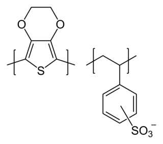
poly(3,4-ethylenedioxythiophene) polystyrene sulfonate (PEDOT:PSS) is a polymer mixture of two ionomers. One component in this mixture is made up of polystyrene sulfonate which is a sulfonated polystyrene. Part of the sulfonyl groups are deprotonated and carry a negative charge. The other component poly(3,4-ethylenedioxythiophene) (PEDOT) is a conjugated polymer and carries positive charges and is based on polythiophene. Together the charged macromolecules form a macromolecular salt.

<span class="mw-page-title-main">Poly(3,4-ethylenedioxythiophene)</span>

Poly(3,4-ethylenedioxythiophene) is a conducting polymer based on 3,4-ethylenedioxythiophene or EDOT. It was first reported by Bayer AG in 1989.

Hybrid solar cells combine advantages of both organic and inorganic semiconductors. Hybrid photovoltaics have organic materials that consist of conjugated polymers that absorb light as the donor and transport holes. Inorganic materials in hybrid cells are used as the acceptor and electron transporter in the structure. The hybrid photovoltaic devices have a potential for not only low-cost by roll-to-roll processing but also for scalable solar power conversion.

<span class="mw-page-title-main">Indium(III) oxide</span> Chemical compound

Indium(III) oxide (In2O3) is a chemical compound, an amphoteric oxide of indium.

<span class="mw-page-title-main">Potential applications of carbon nanotubes</span>

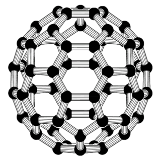
Carbon nanotubes (CNTs) are cylinders of one or more layers of graphene (lattice). Diameters of single-walled carbon nanotubes (SWNTs) and multi-walled carbon nanotubes (MWNTs) are typically 0.8 to 2 nm and 5 to 20 nm, respectively, although MWNT diameters can exceed 100 nm. CNT lengths range from less than 100 nm to 0.5 m.

<span class="mw-page-title-main">PEDOT-TMA</span> Chemical compound

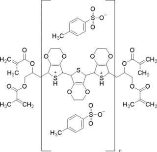
Poly(3,4-ethylenedioxythiophene)-tetramethacrylate or PEDOT-TMA is a p-type conducting polymer based on 3,4-ethylenedioxylthiophene or the EDOT monomer. It is a modification of the PEDOT structure. Advantages of this polymer relative to PEDOT are that it is dispersible in organic solvents, and it is non-corrosive. PEDOT-TMA was developed under a contract with the National Science Foundation, and it was first announced publicly on April 12, 2004. The trade name for PEDOT-TMA is Oligotron. PEDOT-TMA was featured in an article entitled "Next Stretch for Plastic Electronics" that appeared in Scientific American in 2004. The U.S. Patent office issued a patent protecting PEDOT-TMA on April 22, 2008.

Organic photovoltaic devices (OPVs) are fabricated from thin films of organic semiconductors, such as polymers and small-molecule compounds, and are typically on the order of 100 nm thick. Because polymer based OPVs can be made using a coating process such as spin coating or inkjet printing, they are an attractive option for inexpensively covering large areas as well as flexible plastic surfaces. A promising low cost alternative to conventional solar cells made of crystalline silicon, there is a large amount of research being dedicated throughout industry and academia towards developing OPVs and increasing their power conversion efficiency.

<span class="mw-page-title-main">Ultrasonic nozzle</span> Type of spray nozzle

Ultrasonic nozzles are a type of spray nozzle that use high frequency vibrations produced by piezoelectric transducers acting upon the nozzle tip that create capillary waves in a liquid film. Once the amplitude of the capillary waves reaches a critical height, they become too tall to support themselves and tiny droplets fall off the tip of each wave resulting in atomization.

<span class="mw-page-title-main">Organic solar cell</span> Type of photovoltaic

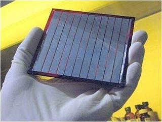
An organic solar cell (OSC) or plastic solar cell is a type of photovoltaic that uses organic electronics, a branch of electronics that deals with conductive organic polymers or small organic molecules, for light absorption and charge transport to produce electricity from sunlight by the photovoltaic effect. Most organic photovoltaic cells are polymer solar cells.

<span class="mw-page-title-main">Copper indium gallium selenide solar cell</span>

A copper indium gallium selenide solar cell is a thin-film solar cell used to convert sunlight into electric power. It is manufactured by depositing a thin layer of copper indium gallium selenide solid solution on glass or plastic backing, along with electrodes on the front and back to collect current. Because the material has a high absorption coefficient and strongly absorbs sunlight, a much thinner film is required than of other semiconductor materials.

<span class="mw-page-title-main">Solar cell research</span> Research in the field of photovoltaics

There are currently many research groups active in the field of photovoltaics in universities and research institutions around the world. This research can be categorized into three areas: making current technology solar cells cheaper and/or more efficient to effectively compete with other energy sources; developing new technologies based on new solar cell architectural designs; and developing new materials to serve as more efficient energy converters from light energy into electric current or light absorbers and charge carriers.

<span class="mw-page-title-main">Photoconductive atomic force microscopy</span> Type of atomic force microscopy

Photoconductive atomic force microscopy (PC-AFM) is a variant of atomic force microscopy that measures photoconductivity in addition to surface forces.

<span class="mw-page-title-main">Surface chemistry of neural implants</span>

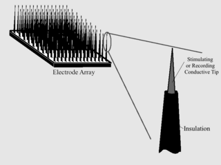
As with any material implanted in the body, it is important to minimize or eliminate foreign body response and maximize effectual integration. Neural implants have the potential to increase the quality of life for patients with such disabilities as Alzheimer's, Parkinson's, epilepsy, depression, and migraines. With the complexity of interfaces between a neural implant and brain tissue, adverse reactions such as fibrous tissue encapsulation that hinder the functionality, occur. Surface modifications to these implants can help improve the tissue-implant interface, increasing the lifetime and effectiveness of the implant.

Vertically aligned carbon nanotube arrays (VANTAs) are a unique microstructure consisting of carbon nanotubes oriented with their longitudinal axis perpendicular to a substrate surface. These VANTAs effectively preserve and often accentuate the unique anisotropic properties of individual carbon nanotubes and possess a morphology that may be precisely controlled. VANTAs are consequently widely useful in a range of current and potential device applications.

<span class="mw-page-title-main">Heterojunction solar cell</span> A solar cell architecture

Heterojunction solar cells (HJT), variously known as Silicon heterojunctions (SHJ) or Heterojunction with Intrinsic Thin Layer (HIT), are a family of photovoltaic cell technologies based on a heterojunction formed between semiconductors with dissimilar band gaps. They are a hybrid technology, combining aspects of conventional crystalline solar cells with thin-film solar cells.

References

  1. 1 2 3 4 Hecht, D. S; Hu; Irvin, G. (2011). "Emerging Transparent Electrodes Based on Thin Films of Carbon Nanotubes, Graphene and Metallic Nanostructures". Advanced Materials. 23 (13): 1482–1513. Bibcode:2011AdM....23.1482H. doi:10.1002/adma.201003188. PMID   21322065. S2CID   197299452.
  2. Manwani, K; Panda, E (2021). "Thickness induced modifications in the valence, conduction bands and optoelectronic properties of undoped and Nb-doped anatase TiO2 thin films". Materials Science in Semiconductor Processing. 134: 106048. doi:10.1016/j.mssp.2021.106048.
  3. Dhakal, Tara, et al. "Transmittance from visible to mid infra-red in AZO films grown by atomic layer deposition system." Solar Energy 86.5 (2012): 1306-1312. | https://doi.org/10.1016/j.solener.2012.01.022
  4. Wan, J; Xu, Y; Ozdemir, B (2017). "Tunable Broadband Nanocarbon Transparent Conductor by Electrochemical Intercalation". ACS Nano. 11 (1): 788–796. Bibcode:2017Nano...11..788W. doi:10.1021/acsnano.6b07191. PMID   28033469.
  5. Gao, Jinwei (February 12, 2014). "Uniform Self-Forming Metallic Network as a High-Performance Transparent Conductive Electrode". Advanced Materials. 26 (6): 873–877. Bibcode:2014AdM....26..873H. doi:10.1002/adma.201302950. PMID   24510662. S2CID   205251636.
  6. Gao, Jinwei (28 November 2014). "Bio-inspired networks for optoelectronic applications". Nature Communications. 5 (5674): 5674. Bibcode:2014NatCo...5.5674H. doi: 10.1038/ncomms6674 . PMID   25430671.
  7. Gao, Jinwei (26 September 2016). "Optimization of hierarchical structure and nanoscale-enabled plasmonic refraction for window electrodes in photovoltaics". Nature Communications. 7 (12825): 12825. Bibcode:2016NatCo...712825H. doi:10.1038/ncomms12825. PMC   5052667 . PMID   27667099.
  8. Wu, Zhuangchun, et al. "Transparent, conductive carbon nanotube films." Science 305.5688 (2004): 1273-1276.
  9. Ren, Xingang (2015). "Optically enhanced semi-transparent organic solar cells through hybrid metal/nanoparticle/dielectric nanostructure". Nano Energy. 17: 187–195. doi:10.1016/j.nanoen.2015.08.014.
  10. Conductive Oxide Thin Films Archived 2013-10-03 at the Wayback Machine Materion Technical Paper, "Transparent Conductive Oxide Thin Films"
  11. Swallow, J. E. N.; et al. (2017). "Self-compensation in transparent conducting F-doped SnO2". Advanced Functional Materials. 28 (4): 1701900. doi: 10.1002/adfm.201701900 .
  12. Manwani, K; Panda, E (2021). "Thickness induced modifications in the valence, conduction bands and optoelectronic properties of undoped and Nb-doped anatase TiO2 thin films". Materials Science in Semiconductor Processing. 134: 106048. doi:10.1016/j.mssp.2021.106048.
  13. 1 2 3 Minami, Tadatsugu (2005). "Transparent conducting oxide semiconductors for transparent electrodes". Semiconductor Science and Technology. 20 (4): S35–S44. Bibcode:2005SeScT..20S..35M. doi:10.1088/0268-1242/20/4/004. S2CID   93242002.
  14. Dominici, L; Michelotti, F; Brown, TM; et al. (2009). "Plasmon polaritons in the near infrared on fluorine doped tin oxide films". Optics Express. 17 (12): 10155–67. Bibcode:2009OExpr..1710155D. doi: 10.1364/OE.17.010155 . PMID   19506669.
  15. Chen, Zhangxian (2013). "Fabrication of Highly Transparent and Conductive Indium–Tin Oxide Thin Films with a High Figure of Merit via Solution Processing". Langmuir. 29 (45): 13836–13842. doi:10.1021/la4033282. PMID   24117323.
  16. Indium Price Supported by LCD Demand and New Uses for the Metal
  17. Swallow, J.E.N.; et al. (September 2019). "Resonant doping for high mobility transparent conductors". Materials Horizons. doi: 10.1039/c9mh01014a .
  18. Williamson, B.A.D.; et al. (February 2020). "Resonant Ta Doping for Enhanced Mobility in Transparent Conducting SnO2". Chemistry of Materials. 32 (5): 1964–1973. doi: 10.1021/acs.chemmater.9b04845 . PMC   7147269 . PMID   32296264.
  19. Young-Hui Koa, Ju-Won Leeb, Won-Kook Choic, Sung-Ryong Kim, 2014, "Ultrasonic Sprayed Graphene Oxide and Air Sprayed Ag Nanowire for the Preparation of Flexible Transparent Conductive Films," The Chemical Society of Japan
  20. Indium, USGS report
  21. 1 2 Edwards, P. P.; Porch, A.; Jones, M. O.; Morgan, D. V.; Perks, R. M. (2004). "Basic materials physics of transparent conducting oxides". Dalton Transactions (19): 2995–3002. doi:10.1039/b408864f. PMID   15452622.
  22. The Nobel Prize in Chemistry, 2000: Conductive polymers
  23. "Historical Background (or there is nothing new under the Sun)" in György Inzelt "Conducting Polymers" Springer, 2008, Berlin, Heidelberg. doi : 10.1007/978-3-540-75930-0
  24. Hush, Noel S. (2003). "An Overview of the First Half-Century of Molecular Electronics". Annals of the New York Academy of Sciences. 1006 (1): 1–20. Bibcode:2003NYASA1006....1H. doi:10.1196/annals.1292.016. PMID   14976006. S2CID   24968273.
  25. Skotheim, Terje A. Reynold, John "Handbook of Conducting Polymers" CRC Press, 1998 ISBN   0-8247-0050-3
  26. Pregan, B; Gratzel, M (1991). "A low-cost, high-efficiency solar cell based on dye-sensitized colloidal TiO2 films". Nature. 353 (6346): 737–740. Bibcode:1991Natur.353..737O. doi:10.1038/353737a0. S2CID   4340159.
  27. Hu, Liangbing; Hecht, David S.; Grüner, George (2009). "Infrared transparent carbon nanotube thin films". Applied Physics Letters. 94 (8): 081103. Bibcode:2009ApPhL..94h1103H. doi:10.1063/1.3075067.
  28. 1 2 3 Groenendaal, L.; Jonas, F.; Freitag, D.; Pielartzik, H.; Reynolds, J. R. (2000). "Poly(3,4-ethylenedioxythiophene) and Its Derivatives: Past, Present, and Future". Advanced Materials. 12 (7): 481–494. doi:10.1002/(SICI)1521-4095(200004)12:7<481::AID-ADMA481>3.0.CO;2-C.
  29. Saghaei, Jaber; Fallahzadeh, Ali; Saghaei, Tayebeh (September 2015). "ITO-free organic solar cells using highly conductive phenol-treated PEDOT:PSS anodes". Organic Electronics. 24: 188–194. doi:10.1016/j.orgel.2015.06.002.
  30. Louwet, F; Groenendaal, L.; Dhaen, J.; Manca, J.; Van Luppen, J.; Verdonck, E.; Leenders, L. (2003). "PEDOT/PSS: synthesis, characterization, properties and applications". Synthetic Metals. 135–136: 115–117. doi:10.1016/S0379-6779(02)00518-0.
  31. 1 2 Ouyang, J.; Chu, C.-W.; Chen, F.-C.; Xu, Q.; Yang, Y. (2005). "High-Conductivity Poly(3,4-ethylenedioxythiophene):Poly(styrene sulfonate) Film and Its Application in Polymer Optoelectronic Devices". Advanced Functional Materials. 15 (2): 203–208. doi: 10.1002/adfm.200400016 . S2CID   95522337.
  32. Worfolk, Brian J.; Andrews, Sean C.; Park, Steve; Reinspach, Julia; Liu, Nan; Toney, Michael F.; Mannsfeld, Stefan C. B.; Bao, Zhenan (2015-11-17). "Ultrahigh electrical conductivity in solution-sheared polymeric transparent films". Proceedings of the National Academy of Sciences. 112 (46): 14138–14143. Bibcode:2015PNAS..11214138W. doi: 10.1073/pnas.1509958112 . ISSN   0027-8424. PMC   4655535 . PMID   26515096.
  33. 1 2 Coppo, P; Schroeder, Raoul; Grell, Martin; Turner, Michael L (2004). "Investigation of solution processed poly(4,4-dioctyl cyclopentadithiophene) thin films as transparent conductors". Synthetic Metals. 143 (2): 203–206. doi:10.1016/j.synthmet.2003.12.001.
  34. Hong, Seunghun; Myung, Sung (2007). "Nanotube Electronics: A flexible approach to mobility". Nature Nanotechnology. 2 (4): 207–8. Bibcode:2007NatNa...2..207H. doi:10.1038/nnano.2007.89. PMID   18654263.
  35. Green, Alexander A.; Hersam, Mark C. (2008). "Colored Semitransparent Conductive Coatings Consisting of Monodisperse Metallic Single-Walled Carbon Nanotubes". Nano Letters. 8 (5): 1417–22. Bibcode:2008NanoL...8.1417G. doi:10.1021/nl080302f. PMID   18393537.
  36. Lonaker, Ganesh S.; Mahajan, Mrunal S.; Ghosh, Sanjay S.; Sali, Jaydeep V. (2012). "Modeling thin film formation by Ultrasonic Spray Method: A case of PEDOT:PSS thin films". Organic Electronics. 13 (11): 2575–2581. doi:10.1016/j.orgel.2012.07.013.
  37. Steirer, K. Xerxes; Reese, Matthew O.; Rupert, Benjamin L.; Kopidakis, Nikos; Olson, Dana C.; Collins, Reuben T.; Ginley, David S. (2008). "Ultrasonic spray deposition for production of organic solar cells" (PDF). Solar Energy Materials & Solar Cells. 93 (4): 447–453. doi:10.1016/j.solmat.2008.10.026.
  38. Contreras, M.A.; Barnes, T.; Vandelagemaat, J.; Rumbles, G.; Coutts, T.J.; Weeks, C.; Glatkowski, P.; Levitsky, I.; et al. (2007). "Replacement of Transparent Conductive Oxides by Single-Wall Carbon Nanotubes in Cu(In,Ga)Se2-Based Solar Cells". Journal of Physical Chemistry C. 111 (38): 14045–14048. doi:10.1021/jp075507b.
  39. Rao, K. D. M.; Gupta, Ritu; Kulkarni, Giridhar U. (2014-05-11). "Fabrication of Large Area, High-Performance, Transparent Conducting Electrodes Using a Spontaneously Formed Crackle Network as Template". Advanced Materials Interfaces. 1 (6): 1400090. doi:10.1002/admi.201400090. ISSN   2196-7350. S2CID   137671656.
  40. Gupta, Ritu; Rao, K. D. M.; Srivastava, Kartikeya; Kumar, Ankush; Kiruthika, S.; Kulkarni, Giridhar U. (2014-07-08). "Spray Coating of Crack Templates for the Fabrication of Transparent Conductors and Heaters on Flat and Curved Surfaces". ACS Applied Materials & Interfaces. 6 (16): 13688–13696. doi:10.1021/am503154z. ISSN   1944-8244. PMID   25001064.
  41. Kumar, Ankush (2017-01-03). "Predicting efficiency of solar cells based on transparent conducting electrodes". Journal of Applied Physics. 121 (1): 014502. Bibcode:2017JAP...121a4502K. doi:10.1063/1.4973117. ISSN   0021-8979.
  42. Rao, K. D. M.; Hunger, Christoph; Gupta, Ritu; Kulkarni, Giridhar U.; Thelakkat, Mukundan (2014). "A cracked polymer templated metal network as a transparent conducting electrode for ITO-free organic solar cells". Phys. Chem. Chem. Phys. 16 (29): 15107–15110. Bibcode:2014PCCP...1615107R. doi: 10.1039/C4CP02250E . ISSN   1463-9076. PMID   24958552.