Selected area diffraction

Last updated
SADP of a single austenite crystal in a piece of steel Austenite ZADP.jpg
SADP of a single austenite crystal in a piece of steel

Selected area (electron) diffraction (abbreviated as SAD or SAED) is a crystallographic experimental technique typically performed using a transmission electron microscope (TEM). It is a specific case of electron diffraction used primarily in material science and solid state physics as one of the most common experimental techniques. Especially with appropriate analytical software, SAD patterns (SADP) can be used to determine crystal orientation, measure lattice constants or examine its defects.

Contents

Principle

In transmission electron microscope, a thin crystalline sample is illuminated by parallel beam of electrons accelerated to energy of hundreds of kiloelectron volts. At these energies samples are transparent for the electrons if the sample is thinned enough (typically less than 100  nm). Due to the wave–particle duality, the high-energetic electrons behave as matter waves with wavelength of a few thousandths of a nanometer. The relativistic wavelength is given by

where is Planck's constant, is the electron rest mass, is the elementary charge, is the speed of light and is an electric potential accelerating the electrons (also called acceleration voltage). [1] For instance the acceleration voltage of 200 kV results in a wavelength of 2.508 pm. [2]

Normally incident electron beam is transmitted (
n
{\displaystyle n}
=1) and diffracted under specific angles (
n
{\displaystyle n}
equal to 1 and 2). Diffraction on crystal lattice.png
Normally incident electron beam is transmitted (=1) and diffracted under specific angles ( equal to 1 and 2).

Since the spacing between atoms in crystals is about a hundred times larger, the electrons are diffracted on the crystal lattice, acting as a diffraction grating. Due to the diffraction, part of the electrons is scattered at particular angles (diffracted beams), while others pass through the sample without changing their direction (transmitted beams). In order to determine the diffraction angles, the electron beam normally incident to the atomic lattice can be seen as a planar wave, which is re-transmitted by each atom as a spherical wave. Due to the constructive interference, the spherical waves from number of diffracted beams under angles given, approximately, by the Bragg condition

where the integer is an order of diffraction and is the distance between atoms (if only one row of atoms is assumed as in the illustration aside) or a distance between atomic planes parallel to the beam (in a real 3D atomic structure). For finite samples this equation is only approximately correct.

Imaging scheme of magnetic lens (center) with magnified image (left) and diffraction pattern (right) formed in back focal plane ElmagLensScheme.png
Imaging scheme of magnetic lens (center) with magnified image (left) and diffraction pattern (right) formed in back focal plane

After being deflected by the microscope's magnetic lens, each set of initially parallel beams intersect in the back focal plane forming the diffraction pattern. The transmitted beams intersect right in the optical axis. The diffracted beams intersect at certain distance from the optical axis (corresponding to interplanar distance of the planes diffracting the beams) and under certain azimuth (corresponding to the orientation of the planes diffracting the beams). This allows to form a pattern of bright spots typical for SAD. [3]

Relation between spot and ring diffraction illustrated on 1 to 1000 grains of MgO using simulation engine of CrysTBox. Experimental image shown below. SpotToRingDiffraction.gif
Relation between spot and ring diffraction illustrated on 1 to 1000 grains of MgO using simulation engine of CrysTBox. Experimental image shown below.

SAD is called "selected" because it allows the user to select the sample area from which the diffraction pattern will be acquired. For this purpose, there is a selected area aperture located below the sample holder. It is a metallic sheet with several differently sized holes which can be inserted into the beam. The user can select the aperture of appropriate size and position it so that it only allows to pass the portion of beam corresponding to the selected area. Therefore, the resulting diffraction pattern will only reflect the area selected by the aperture. This allows to study small objects such as crystallites in polycrystalline material with a broad parallel beam.

Character of the resulting diffraction image depends on whether the beam is diffracted by one single crystal or by number of differently oriented crystallites for instance in a polycrystalline material. The single-crystalline diffractogram depicts a regular pattern of bright spots. This pattern can be seen as a two-dimensional projection of reciprocal crystal lattice. If there are more contributing crystallites, the diffraction image becomes a superposition of individual crystals' diffraction patterns. Ultimately, this superposition contains diffraction spots of all possible crystallographic plane systems in all possible orientations. For two reasons, these conditions result in a diffractogram of concentric rings:

  1. There are discrete spacings between various parallel crystallographic planes and therefore the beams satisfying the diffraction condition can only form diffraction spots in discrete distances from the transmitted beam.
  2. There are all possible orientations of crystallographic planes and therefore the diffraction spots are formed around the transmitted beam in the whole 360-degree azimuthal range.

Interpretation and analysis

Single-crystalline SADP automatically interpreted with CrysTBox software. DiffractGUI.png
Single-crystalline SADP automatically interpreted with CrysTBox software.

SAD analysis is widely used in material research for its relative simplicity and high information value. Once the sample is prepared and examined in a modern transmission electron microscope, the device allows for a routine diffraction acquisition in a matter of seconds. If the images are interpreted correctly, they can be used to identify crystal structures, determine their orientations, measure crystal characteristics, examine crystal defects or material textures. The course of analysis depends on whether the diffractogram depicts ring or spot diffraction pattern and on the quantity to be determined.

Software tools based on computer vision algorithms simplifies quantitative analysis. [4]

Spot diffraction pattern

If the SAD is taken from one a or a few single crystals, the diffractogram depicts a regular pattern of bright spots. Since the diffraction pattern can be seen as a two-dimensional projection of reciprocal crystal lattice, the pattern can be used to measure lattice constants, specifically the distances and angles between crystallographic planes. The lattice parameters are typically distinctive for various materials and their phases which allows to identify the examined material or at least differentiate between possible candidates.

Diffraction pattern of magnesium simulated using CrysTBox for various crystal orientations. Crystal orientation and diffraction.gif
Diffraction pattern of magnesium simulated using CrysTBox for various crystal orientations.

Even though the SAD-based analyses were not considered quantitative for a long time, computer tools brought accuracy and repeatability allowing to routinely perform accurate measurements of interplanar distances or angles on appropriately calibrated microscopes. Tools such as CrysTBox are capable of automated analysis achieving sub-pixel precision. [4]

If the sample is tilted against the electron beam, diffraction conditions are satisfied for different set of crystallographic planes yielding different constellation of diffraction spots. This allows to determine the crystal orientation, which can be used for instance to set up the orientation needed for particular experiment, to determine misorientation between adjacent grains or crystal twins. [2] [4] Since different sample orientations provide different projections of the reciprocal lattice, they provide an opportunity to reconstruct the three-dimensional information lost in individual projections. A series of diffractograms varying in tilt can be acquired and processed with diffraction tomography analysis in order to reconstruct an unknown crystal structure. [5]

SAD can also be used to analyze crystal defects such as stacking faults.

Ring diffraction pattern

RingGUI input.png
RingGUI quadrant.png
Ring diffraction image of MgO as recorded (left) and processed with CrysTBox ringGUI (right).

If the illuminated area selected by the aperture covers many differently oriented crystallites, their diffraction patterns superimpose forming an image of concentric rings. The ring diffractogram is typical for polycrystalline samples, powders or nanoparticles. Diameter of each ring corresponds to interplanar distance of a plane system present in the sample. Instead of information about individual grains or the sample orientation, this diffractogram provides more of a statistical information for instance about overall crystallinity or texture. Textured materials are characteristic by a non-uniform intensity distribution along the ring circumference despite crystallinity sufficient for generating smooth rings. Ring diffractograms can be also used to discriminate between nanocrystalline and amorphous phases. [2]

Not all the features depicted in the diffraction image are necessarily wanted. The transmitted beam is often too strong and needs to be shadowed with a beam-stopper in order to protect the camera. The beam-stopper typically shadows part of the useful information as well. Towards the rings center, the background intensity also gradually increases lowering the contrast of diffraction rings. Modern analytical software allows to minimize such unwanted image features and together with other functionalities improves the image readability it helps with image interpretation. [4]

Relation to other techniques

Diffraction patterns with different crystallinity and beam convergence. From left: spot diffraction (SAD), CBED, ring diffraction (SAD) Difrakce.png
Diffraction patterns with different crystallinity and beam convergence. From left: spot diffraction (SAD), CBED, ring diffraction (SAD)

An SADP is acquired under parallel electron illumination. In the case of convergent beam, a convergent beam electron diffraction (CBED) is achieved. [6] [3] The beam used in SAD is broad illuminating a wide sample area. In order to analyze only a specific sample area, the selected area aperture in the image plane is used. This is in contrast with nanodiffraction, where the site-selectivity is achieved using a beam condensed to a narrow probe. [3] SAD is important in direct imaging for instance when orienting the sample for high resolution microscopy or setting up dark-field imaging conditions.

High-resolution electron microscope images can be transformed into an artificial diffraction pattern using Fourier transform. Then, they can be processed the same way as real diffractograms allowing to determine crystal orientation, measure interplanar angles and distances even with picometric precision. [7]

SAD is similar to X-ray diffraction, but unique in that areas as small as several hundred nanometers in size can be examined, whereas X-ray diffraction typically samples areas much larger.

See also

Related Research Articles

<span class="mw-page-title-main">Crystallography</span> Scientific study of crystal structures

Crystallography is the experimental science of determining the arrangement of atoms in crystalline solids. Crystallography is a fundamental subject in the fields of materials science and solid-state physics. The word crystallography is derived from the Ancient Greek word κρύσταλλος, with its meaning extending to all solids with some degree of transparency, and γράφειν. In July 2012, the United Nations recognised the importance of the science of crystallography by proclaiming that 2014 would be the International Year of Crystallography.

<span class="mw-page-title-main">Transmission electron microscopy</span> Imaging and diffraction using electrons that pass through samples

Transmission electron microscopy (TEM) is a microscopy technique in which a beam of electrons is transmitted through a specimen to form an image. The specimen is most often an ultrathin section less than 100 nm thick or a suspension on a grid. An image is formed from the interaction of the electrons with the sample as the beam is transmitted through the specimen. The image is then magnified and focused onto an imaging device, such as a fluorescent screen, a layer of photographic film, or a detector such as a scintillator attached to a charge-coupled device or a direct electron detector.

<span class="mw-page-title-main">Electron diffraction</span> Bending of electron beams due to electrostatic interactions with matter

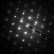
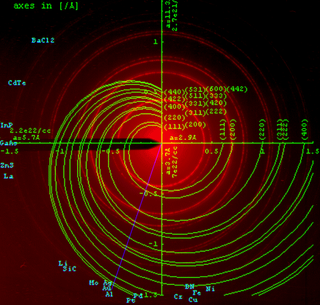
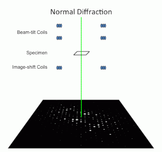
Electron diffraction is a generic term for phenomena associated with changes in the direction of electron beams due to elastic interactions with atoms. It occurs due to elastic scattering, when there is no change in the energy of the electrons. The negatively charged electrons are scattered due to Coulomb forces when they interact with both the positively charged atomic core and the negatively charged electrons around the atoms. The resulting map of the directions of the electrons far from the sample is called a diffraction pattern, see for instance Figure 1. Beyond patterns showing the directions of electrons, electron diffraction also plays a major role in the contrast of images in electron microscopes.

Reflection high-energy electron diffraction (RHEED) is a technique used to characterize the surface of crystalline materials. RHEED systems gather information only from the surface layer of the sample, which distinguishes RHEED from other materials characterization methods that also rely on diffraction of high-energy electrons. Transmission electron microscopy, another common electron diffraction method samples mainly the bulk of the sample due to the geometry of the system, although in special cases it can provide surface information. Low-energy electron diffraction (LEED) is also surface sensitive, but LEED achieves surface sensitivity through the use of low energy electrons.

<span class="mw-page-title-main">Electron backscatter diffraction</span> Scanning electron microscopy technique

Electron backscatter diffraction (EBSD) is a scanning electron microscopy (SEM) technique used to study the crystallographic structure of materials. EBSD is carried out in a scanning electron microscope equipped with an EBSD detector comprising at least a phosphorescent screen, a compact lens and a low-light camera. In the microscope an incident beam of electrons hits a tilted sample. As backscattered electrons leave the sample, they interact with the atoms and are both elastically diffracted and lose energy, leaving the sample at various scattering angles before reaching the phosphor screen forming Kikuchi patterns (EBSPs). The EBSD spatial resolution depends on many factors, including the nature of the material under study and the sample preparation. They can be indexed to provide information about the material's grain structure, grain orientation, and phase at the micro-scale. EBSD is used for impurities and defect studies, plastic deformation, and statistical analysis for average misorientation, grain size, and crystallographic texture. EBSD can also be combined with energy-dispersive X-ray spectroscopy (EDS), cathodoluminescence (CL), and wavelength-dispersive X-ray spectroscopy (WDS) for advanced phase identification and materials discovery.

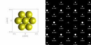
Electron crystallography is a method to determine the arrangement of atoms in solids using a transmission electron microscope (TEM). It can involve the use of high-resolution transmission electron microscopy images, electron diffraction patterns including convergent-beam electron diffraction or combinations of these. It has been successful in determining some bulk structures, and also surface structures. Two related methods are low-energy electron diffraction which has solved the structure of many surfaces, and reflection high-energy electron diffraction which is used to monitor surfaces often during growth.

<span class="mw-page-title-main">Powder diffraction</span>

Powder diffraction is a scientific technique using X-ray, neutron, or electron diffraction on powder or microcrystalline samples for structural characterization of materials. An instrument dedicated to performing such powder measurements is called a powder diffractometer.

A pole figure is a graphical representation of the orientation of objects in space. For example, pole figures in the form of stereographic projections are used to represent the orientation distribution of crystallographic lattice planes in crystallography and texture analysis in materials science.

<span class="mw-page-title-main">High-resolution transmission electron microscopy</span>

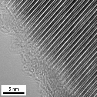
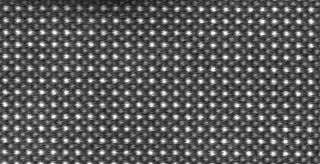
High-resolution transmission electron microscopy is an imaging mode of specialized transmission electron microscopes that allows for direct imaging of the atomic structure of samples. It is a powerful tool to study properties of materials on the atomic scale, such as semiconductors, metals, nanoparticles and sp2-bonded carbon. While this term is often also used to refer to high resolution scanning transmission electron microscopy, mostly in high angle annular dark field mode, this article describes mainly the imaging of an object by recording the two-dimensional spatial wave amplitude distribution in the image plane, similar to a "classic" light microscope. For disambiguation, the technique is also often referred to as phase contrast transmission electron microscopy, although this term is less appropriate. At present, the highest point resolution realised in high resolution transmission electron microscopy is around 0.5 ångströms (0.050 nm). At these small scales, individual atoms of a crystal and defects can be resolved. For 3-dimensional crystals, it is necessary to combine several views, taken from different angles, into a 3D map. This technique is called electron tomography.

<span class="mw-page-title-main">Dark-field microscopy</span> Laboratory technique

Dark-field microscopy describes microscopy methods, in both light and electron microscopy, which exclude the unscattered beam from the image. Consequently, the field around the specimen is generally dark.

Diffraction topography is a imaging technique based on Bragg diffraction. Diffraction topographic images ("topographies") record the intensity profile of a beam of X-rays diffracted by a crystal. A topography thus represents a two-dimensional spatial intensity mapping of reflected X-rays, i.e. the spatial fine structure of a Laue reflection. This intensity mapping reflects the distribution of scattering power inside the crystal; topographs therefore reveal the irregularities in a non-ideal crystal lattice. X-ray diffraction topography is one variant of X-ray imaging, making use of diffraction contrast rather than absorption contrast which is usually used in radiography and computed tomography (CT). Topography is exploited to a lesser extends with neutrons, and has similarities to dark field imaging in the electron microscope community.

<span class="mw-page-title-main">Kikuchi lines (physics)</span> Patterns formed by scattering

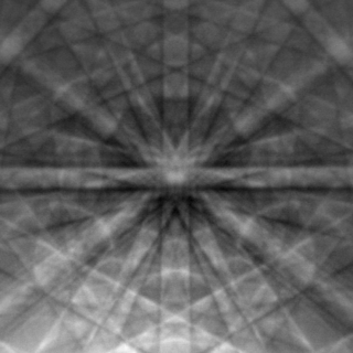
Kikuchi lines are patterns of electrons formed by scattering. They pair up to form bands in electron diffraction from single crystal specimens, there to serve as "roads in orientation-space" for microscopists uncertain of what they are looking at. In transmission electron microscopes, they are easily seen in diffraction from regions of the specimen thick enough for multiple scattering. Unlike diffraction spots, which blink on and off as one tilts the crystal, Kikuchi bands mark orientation space with well-defined intersections as well as paths connecting one intersection to the next.

A crystallographic database is a database specifically designed to store information about the structure of molecules and crystals. Crystals are solids having, in all three dimensions of space, a regularly repeating arrangement of atoms, ions, or molecules. They are characterized by symmetry, morphology, and directionally dependent physical properties. A crystal structure describes the arrangement of atoms, ions, or molecules in a crystal.

<span class="mw-page-title-main">Zone axis</span> High symmetry orientation of a crystal

Zone axis, a term sometimes used to refer to "high-symmetry" orientations in a crystal, most generally refers to any direction referenced to the direct lattice of a crystal in three dimensions. It is therefore indexed with direct lattice indices, instead of with Miller indices.

<span class="mw-page-title-main">Geometric phase analysis</span> Method of digital signal processing

Geometric phase analysis is a method of digital signal processing used to determine crystallographic quantities such as d-spacing or strain from high-resolution transmission electron microscope images. The analysis needs to be performed using specialized computer program.

<span class="mw-page-title-main">Precession electron diffraction</span> Averaging technique for electron diffraction

Precession electron diffraction (PED) is a specialized method to collect electron diffraction patterns in a transmission electron microscope (TEM). By rotating (precessing) a tilted incident electron beam around the central axis of the microscope, a PED pattern is formed by integration over a collection of diffraction conditions. This produces a quasi-kinematical diffraction pattern that is more suitable as input into direct methods algorithms to determine the crystal structure of the sample.

<span class="mw-page-title-main">Convergent beam electron diffraction</span> Convergent beam electron diffraction technique

Convergent beam electron diffraction (CBED) is an electron diffraction technique where a convergent or divergent beam of electrons is used to study materials.

<span class="mw-page-title-main">CrysTBox</span> Free crystallographic software

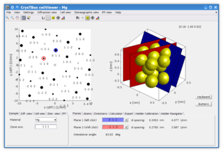
CrysTBox is a suite of computer tools designed to accelerate material research based on transmission electron microscope images via highly accurate automated analysis and interactive visualization. Relying on artificial intelligence and computer vision, CrysTBox makes routine crystallographic analyses simpler, faster and more accurate compared to human evaluators. The high level of automation together with sub-pixel precision and interactive visualization makes the quantitative crystallographic analysis accessible even for non-crystallographers allowing for an interdisciplinary research. Simultaneously, experienced material scientists can take advantage of advanced functionalities for comprehensive analyses.

Transmission Kikuchi Diffraction (TKD), also sometimes called transmission-electron backscatter diffraction (t-EBSD), is a method for orientation mapping at the nanoscale. It’s used for analysing the microstructures of thin transmission electron microscopy (TEM) specimens in the scanning electron microscope (SEM). This technique has been widely utilised in the characterization of nano-crystalline materials, including oxides, superconductors, and metallic alloys.

<span class="mw-page-title-main">Weak-beam dark-field microscopy</span> Electron microscopy technique

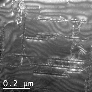
Weak beam dark field (WBDF) microscopy is a type of transmission electron microscopy (TEM) dark field imaging technique that allows for the visualization of crystal defects with high resolution and contrast. Specifically, the technique is mainly used to study crystal defects such as dislocations, stacking faults, and interfaces in crystalline materials. WBDF is a valuable tool for studying the microstructure of materials, as it can provide detailed information about the nature and distribution of defects in crystals. These characteristics can have a significant impact on material properties such as strength, ductility, and corrosion resistance.

References

  1. Kirkland, Earl (2010). Advanced computing in electron microscopy. New York: Springer. ISBN   978-1-4419-6533-2. OCLC   668095602.
  2. 1 2 3 De Graef, Marc (2003-03-27). Introduction to Conventional Transmission Electron Microscopy. Cambridge University Press. doi:10.1017/cbo9780511615092. ISBN   978-0-521-62006-2.
  3. 1 2 3 Fultz, B (2013). Transmission electron microscopy and diffractometry of materials. Heidelberg New York: Springer. ISBN   978-3-642-43315-3. OCLC   796932144.
  4. 1 2 3 4 Klinger, Miloslav (2017-07-07). "More features, more tools, more CrysTBox". Journal of Applied Crystallography. International Union of Crystallography (IUCr). 50 (4): 1226–1234. Bibcode:2017JApCr..50.1226K. doi:10.1107/s1600576717006793. ISSN   1600-5767.
  5. Gemmi, Mauro; Mugnaioli, Enrico; Gorelik, Tatiana E.; Kolb, Ute; Palatinus, Lukas; Boullay, Philippe; Hovmöller, Sven; Abrahams, Jan Pieter (2019-07-19). "3D Electron Diffraction: The Nanocrystallography Revolution". ACS Central Science. American Chemical Society (ACS). 5 (8): 1315–1329. doi:10.1021/acscentsci.9b00394. ISSN   2374-7943. PMC   6716134 . PMID   31482114.
  6. Morniroli, Jean Paul (2004). Large-Angle Convergent-Beam Electron Diffraction Applications to Crystal Defects. Taylor & Francis. doi:10.1201/9781420034073. ISBN   978-2-901483-05-2.
  7. Klinger, Miloslav; Polívka, Leoš; Jäger, Aleš; Tyunina, Marina (2016-04-12). "Quantitative analysis of structural inhomogeneity in nanomaterials using transmission electron microscopy". Journal of Applied Crystallography. International Union of Crystallography (IUCr). 49 (3): 762–770. Bibcode:2016JApCr..49..762K. doi:10.1107/s1600576716003800. ISSN   1600-5767.