
An integrated circuit or monolithic integrated circuit is a set of electronic circuits on one small flat piece of semiconductor material, usually silicon. Large numbers of miniaturized transistors and other electronic components are integrated together on the chip. This results in circuits that are orders of magnitude smaller, faster, and less expensive than those constructed of discrete components, allowing a large transistor count. The IC's mass production capability, reliability, and building-block approach to integrated circuit design has ensured the rapid adoption of standardized ICs in place of designs using discrete transistors. ICs are now used in virtually all electronic equipment and have revolutionized the world of electronics. Computers, mobile phones and other home appliances are now inextricable parts of the structure of modern societies, made possible by the small size and low cost of ICs such as modern computer processors and microcontrollers.

Semiconductor device fabrication is the process used to manufacture semiconductor devices, typically integrated circuits (ICs) such as computer processors, microcontrollers, and memory chips that are present in everyday electrical and electronic devices. It is a multiple-step photolithographic and physio-chemical process during which electronic circuits are gradually created on a wafer, typically made of pure single-crystal semiconducting material. Silicon is almost always used, but various compound semiconductors are used for specialized applications.
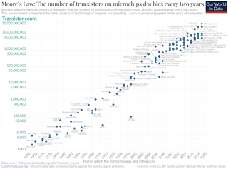
Moore's law is the observation that the number of transistors in an integrated circuit (IC) doubles about every two years. Moore's law is an observation and projection of a historical trend. Rather than a law of physics, it is an empirical relationship linked to gains from experience in production.

Fairchild Semiconductor International, Inc. was an American semiconductor company based in San Jose, California. Founded in 1957 as a division of Fairchild Camera and Instrument, it became a pioneer in the manufacturing of transistors and of integrated circuits. Schlumberger bought the firm in 1979 and sold it to National Semiconductor in 1987; Fairchild was spun off as an independent company again in 1997. In September 2016, Fairchild was acquired by ON Semiconductor.
The semiconductor industry is the aggregate of companies engaged in the design and fabrication of semiconductors and semiconductor devices, such as transistors and integrated circuits. It formed around 1960, once the fabrication of semiconductor devices became a viable business. The industry's annual semiconductor sales revenue has since grown to over $481 billion, as of 2018. The semiconductor industry is in turn the driving force behind the wider electronics industry, with annual power electronics sales of £135 billion as of 2011, annual consumer electronics sales expected to reach $2.9 trillion by 2020, tech industry sales expected to reach $5 trillion in 2019, and e-commerce with over $29 trillion in 2017. In 2019, 32.4% of the semiconductor market segment was for networks and communications devices.
SiGe, or silicon–germanium, is an alloy with any molar ratio of silicon and germanium, i.e. with a molecular formula of the form Si1−xGex. It is commonly used as a semiconductor material in integrated circuits (ICs) for heterojunction bipolar transistors or as a strain-inducing layer for CMOS transistors. IBM introduced the technology into mainstream manufacturing in 1989. This relatively new technology offers opportunities in mixed-signal circuit and analog circuit IC design and manufacture. SiGe is also used as a thermoelectric material for high-temperature applications (>700 K).
In semiconductor manufacturing, silicon on insulator (SOI) technology is fabrication of silicon semiconductor devices in a layered silicon–insulator–silicon substrate, to reduce parasitic capacitance within the device, thereby improving performance. SOI-based devices differ from conventional silicon-built devices in that the silicon junction is above an electrical insulator, typically silicon dioxide or sapphire. The choice of insulator depends largely on intended application, with sapphire being used for high-performance radio frequency (RF) and radiation-sensitive applications, and silicon dioxide for diminished short-channel effects in other microelectronics devices. The insulating layer and topmost silicon layer also vary widely with application.

Miniaturization is the trend to manufacture ever smaller mechanical, optical and electronic products and devices. Examples include miniaturization of mobile phones, computers and vehicle engine downsizing. In electronics, the exponential scaling and miniaturization of silicon MOSFETs leads to the number of transistors on an integrated circuit chip doubling every two years, an observation known as Moore's law. This leads to MOS integrated circuits such as microprocessors and memory chips being built with increasing transistor density, faster performance, and lower power consumption, enabling the miniaturization of electronic devices.
The transistor count is the number of transistors in an electronic device. It is the most common measure of integrated circuit complexity. The rate at which MOS transistor counts have increased generally follows Moore's law, which observed that the transistor count doubles approximately every two years. However, being directly proportional to the area of a chip, transistor count does not represent how advanced the corresponding manufacturing technology is: a better indication of this is the transistor density.
RF Micro Devices, was an American company that designed and manufactured high-performance radio frequency systems and solutions for applications that drive wireless and broadband communications. Headquartered in Greensboro, North Carolina, RFMD traded on the NASDAQ under the symbol RFMD. The Company was founded in Greensboro, North Carolina, in 1991. RF Micro has 3500 employees, 1500 of them in Guilford County, North Carolina.
Nanocomputer refers to a computer smaller than the microcomputer, which is smaller than the minicomputer.
The 14 nm process refers to the MOSFET technology node that is the successor to the 22 nm node. The 14 nm was so named by the International Technology Roadmap for Semiconductors (ITRS). Until about 2011, the node following 22 nm was expected to be 16 nm. All 14 nm nodes use FinFET technology, a type of multi-gate MOSFET technology that is a non-planar evolution of planar silicon CMOS technology.

A multigate device, multi-gate MOSFET or multi-gate field-effect transistor (MuGFET) refers to a metal–oxide–semiconductor field-effect transistor (MOSFET) that has more than one gate on a single transistor. The multiple gates may be controlled by a single gate electrode, wherein the multiple gate surfaces act electrically as a single gate, or by independent gate electrodes. A multigate device employing independent gate electrodes is sometimes called a multiple-independent-gate field-effect transistor (MIGFET). The most widely used multi-gate devices are the FinFET and the GAAFET, which are non-planar transistors, or 3D transistors.
Ghavam G. Shahidi is an Iranian-American electrical engineer and IBM Fellow. He is the director of Silicon Technology at the IBM Thomas J Watson Research Center. He is best known for his pioneering work in silicon-on-insulator (SOI) complementary metal–oxide–semiconductor (CMOS) technology since the late 1980s.
A transistor is a semiconductor device with at least three terminals for connection to an electric circuit. In the common case, the third terminal controls the flow of current between the other two terminals. This can be used for amplification, as in the case of a radio receiver, or for rapid switching, as in the case of digital circuits. The transistor replaced the vacuum-tube triode, also called a (thermionic) valve, which was much larger in size and used significantly more power to operate.The first transistor was successfully demonstrated on December 23, 1947, at Bell Laboratories in Murray Hill, New Jersey. Bell Labs was the research arm of American Telephone and Telegraph (AT&T). The three individuals credited with the invention of the transistor were William Shockley, John Bardeen and Walter Brattain. The introduction of the transistor is often considered one of the most important inventions in history.
In semiconductor manufacturing, the International Roadmap for Devices and Systems defines the 5 nm process as the MOSFET technology node following the 7 nm node. In 2020, Samsung and TSMC entered volume production of 5 nm chips, manufactured for companies including Apple, Marvell, Huawei and Qualcomm.

Akira Yoshino is a Japanese chemist. He is a fellow of Asahi Kasei Corporation and a professor at Meijo University in Nagoya. He created the first safe, production-viable lithium-ion battery which became used widely in cellular phones and notebook computers. Yoshino was awarded the Nobel Prize in Chemistry in 2019 alongside M. Stanley Whittingham and John B. Goodenough.
The IEEE International Electron Devices Meeting (IEDM) is an annual micro- and nanoelectronics conference held each December that serves as a forum for reporting technological breakthroughs in the areas of semiconductor and related device technologies, design, manufacturing, physics, modeling and circuit-device interaction.
Robert J. Mears is an English physicist and engineer. In the 1980s, Dr. Mears invented and demonstrated the Erbium Doped Fiber Amplifier (EDFA) with the help of members of the Optoelectronics Research Group led by Alec Gambling and David Payne. In 2001 he founded Atomera, and as CTO led the invention and development of Mears Silicon Technology (MST), a method for improving the mobility and other characteristics of semiconductor devices. Mears has authored and co-authored more than 250 publications and patents, and is co-inventor of 46 granted US patents. He is an Emeritus Fellow of Pembroke College, Cambridge.
In semiconductor manufacturing, the 2 nm process is the next MOSFET die shrink after the 3 nm process node. As of May 2022, TSMC plans to begin risk 2 nm production at the end of 2024 and mass production in 2025; Intel forecasts production in 2024, and South Korean chipmaker Samsung in 2025.