Related Research Articles
An electron microscope is a microscope that uses a beam of accelerated electrons as a source of illumination. As the wavelength of an electron can be up to 100,000 times shorter than that of visible light photons, electron microscopes have a higher resolving power than light microscopes and can reveal the structure of smaller objects. A scanning transmission electron microscope has achieved better than 50 pm resolution in annular dark-field imaging mode and magnifications of up to about 10,000,000× whereas most light microscopes are limited by diffraction to about 200 nm resolution and useful magnifications below 2000×.

A microscope is an instrument used to see objects that are too small to be seen by the naked eye. Microscopy is the science of investigating small objects and structures using such an instrument. Microscopic means invisible to the eye unless aided by a microscope.
Nanotechnology is the use of matter on an atomic, molecular, and supramolecular scale for industrial purposes. The earliest, widespread description of nanotechnology referred to the particular technological goal of precisely manipulating atoms and molecules for fabrication of macroscale products, also now referred to as molecular nanotechnology. A more generalized description of nanotechnology was subsequently established by the National Nanotechnology Initiative, which defined nanotechnology as the manipulation of matter with at least one dimension sized from 1 to 100 nanometers. This definition reflects the fact that quantum mechanical effects are important at this quantum-realm scale, and so the definition shifted from a particular technological goal to a research category inclusive of all types of research and technologies that deal with the special properties of matter which occur below the given size threshold. It is therefore common to see the plural form "nanotechnologies" as well as "nanoscale technologies" to refer to the broad range of research and applications whose common trait is size.

A scanning electron microscope (SEM) is a type of electron microscope that produces images of a sample by scanning the surface with a focused beam of electrons. The electrons interact with atoms in the sample, producing various signals that contain information about the surface topography and composition of the sample. The electron beam is scanned in a raster scan pattern, and the position of the beam is combined with the intensity of the detected signal to produce an image. In the most common SEM mode, secondary electrons emitted by atoms excited by the electron beam are detected using a secondary electron detector. The number of secondary electrons that can be detected, and thus the signal intensity, depends, among other things, on specimen topography. Some SEMs can achieve resolutions better than 1 nanometer.
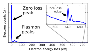
In electron energy loss spectroscopy (EELS) a material is exposed to a beam of electrons with a known, narrow range of kinetic energies. Some of the electrons will undergo inelastic scattering, which means that they lose energy and have their paths slightly and randomly deflected. The amount of energy loss can be measured via an electron spectrometer and interpreted in terms of what caused the energy loss. Inelastic interactions include phonon excitations, inter- and intra-band transitions, plasmon excitations, inner shell ionizations, and Cherenkov radiation. The inner-shell ionizations are particularly useful for detecting the elemental components of a material. For example, one might find that a larger-than-expected number of electrons comes through the material with 285 eV less energy than they had when they entered the material. This is approximately the amount of energy needed to remove an inner-shell electron from a carbon atom, which can be taken as evidence that there is a significant amount of carbon present in the sample. With some care, and looking at a wide range of energy losses, one can determine the types of atoms, and the numbers of atoms of each type, being struck by the beam. The scattering angle can also be measured, giving information about the dispersion relation of whatever material excitation caused the inelastic scattering.
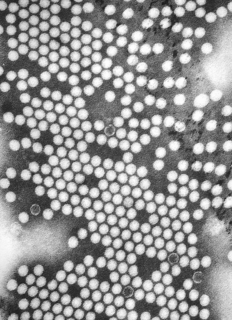
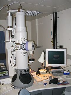
Transmission electron microscopy (TEM) is a microscopy technique in which a beam of electrons is transmitted through a specimen to form an image. The specimen is most often an ultrathin section less than 100 nm thick or a suspension on a grid. An image is formed from the interaction of the electrons with the sample as the beam is transmitted through the specimen. The image is then magnified and focused onto an imaging device, such as a fluorescent screen, a layer of photographic film, or a sensor such as a scintillator attached to a charge-coupled device.

Atomic force microscopy (AFM) or scanning force microscopy (SFM) is a very-high-resolution type of scanning probe microscopy (SPM), with demonstrated resolution on the order of fractions of a nanometer, more than 1000 times better than the optical diffraction-limit.
Since the mid-20th century, electron-beam technology has provided the basis for a variety of novel and specialized applications in semiconductor manufacturing, microelectromechanical systems, nanoelectromechanical systems, and microscopy.
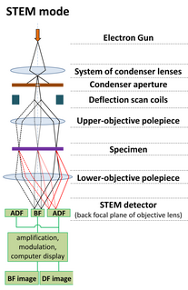
A scanning transmission electron microscope (STEM) is a type of transmission electron microscope (TEM). Pronunciation is [stɛm] or [ɛsti:i:ɛm]. As with a conventional transmission electron microscope (CTEM), images are formed by electrons passing through a sufficiently thin specimen. However, unlike CTEM, in STEM the electron beam is focused to a fine spot which is then scanned over the sample in a raster illumination system constructed so that the sample is illuminated at each point with the beam parallel to the optical axis. The rastering of the beam across the sample makes STEM suitable for analytical techniques such as Z-contrast annular dark-field imaging, and spectroscopic mapping by energy dispersive X-ray (EDX) spectroscopy, or electron energy loss spectroscopy (EELS). These signals can be obtained simultaneously, allowing direct correlation of images and spectroscopic data.

Focused ion beam, also known as FIB, is a technique used particularly in the semiconductor industry, materials science and increasingly in the biological field for site-specific analysis, deposition, and ablation of materials. A FIB setup is a scientific instrument that resembles a scanning electron microscope (SEM). However, while the SEM uses a focused beam of electrons to image the sample in the chamber, a FIB setup uses a focused beam of ions instead. FIB can also be incorporated in a system with both electron and ion beam columns, allowing the same feature to be investigated using either of the beams. FIB should not be confused with using a beam of focused ions for direct write lithography. These are generally quite different systems where the material is modified by other mechanisms.
Plasma etching is a form of plasma processing used to fabricate integrated circuits. It involves a high-speed stream of glow discharge (plasma) of an appropriate gas mixture being shot at a sample. The plasma source, known as etch species, can be either charged (ions) or neutral. During the process, the plasma generates volatile etch products at room temperature from the chemical reactions between the elements of the material etched and the reactive species generated by the plasma. Eventually the atoms of the shot element embed themselves at or just below the surface of the target, thus modifying the physical properties of the target.
Ion-Beam sculpting is a two-step process to make solid-state nanopores. The term itself was coined by Golovchenko and co-workers at Harvard in the paper "Ion-beam sculpting at nanometer length scales." In the process, solid-state nanopores are formed by lateral mass transport about the surface of the substrate, not simply by sputtering, which is the removal of material from the surface.
Gas Cluster Ion Beams (GCIB) is a technology for nano-scale modification of surfaces. It can smooth a wide variety of surface material types to within an angstrom of roughness without subsurface damage. It is also used to chemically alter surfaces through infusion or deposition.

Nanometrology is a subfield of metrology, concerned with the science of measurement at the nanoscale level. Nanometrology has a crucial role in order to produce nanomaterials and devices with a high degree of accuracy and reliability in nanomanufacturing.

The Nano and Micro Devices Center (NMDC) is a research center located at the University of Alabama in Huntsville. The center forms the backbone of nanotechnology research in the university. It operates a level 4 clean room as well as several other lab facilities.
In situ electron microscopy is an investigatory technique where an electron microscope is used to watch a sample's response to a stimulus in real time. Due to the nature of the high-energy beam of electrons used to image a sample in an electron microscope, microscopists have long observed that specimens are routinely changed or damaged by the electron beam. Starting in the 1960s, and using transmission electron microscopes (TEMs), scientists made deliberate attempts to modify materials while the sample was in the specimen chamber, and to capture images through time of the induced damages.

The characterization of nanoparticles is a branch of nanometrology that deals with the characterization, or measurement, of the physical and chemical properties of nanoparticles. Nanoparticles measure less than 100 nanometers in at least one of their external dimensions, and are often engineered for their unique properties. Nanoparticles are unlike conventional chemicals in that their chemical composition and concentration are not sufficient metrics for a complete description, because they vary in other physical properties such as size, shape, surface properties, crystallinity, and dispersion state.
A probe tip in scanning microscopy is a very sharp object made from metal or other materials, like a sewing needle with a point at one end with nano or sub-nanometer order of dimension. It can interact with up to one molecule or atom of a given surface of a sample that can reveal authentic properties of the surface such as morphology, topography, mapping and electrical properties of a single atom or molecule on the surface of the sample.
This glossary of nanotechnology is a list of definitions of terms and concepts relevant to nanotechnology, its sub-disciplines, and related fields.
Ultrafast scanning electron microscopy (UFSEM) is an innovative consolidated facility that combines two microscopic modalities, Pump-probe microscopy and Scanning electron microscope, to gather temporal and spatial resolution phenomena. In fact, this technique is very wonderful at which ultrashort laser will be used forpump excitation of the material and the sample response will be detected by an Everhart-Thornley detector. Acquiring data depends mainly on formation of images by raster scan mode after pumping with short laser pulse at different delay times. The characterization of the output image will be done through the temporal resolution aspect. Thus, the idea is to exploit the shorter DeBroglie wavelength in respect to the photons which has great impact to increase the resolution about 1 nm. That technique is an up-to-date approach to study the dynamic of charge on material surfaces.
References
- 1 2 3 4 5 Baird, Bertram (27 May 2013). "Nanotechnology Reveals Secrets Of CO2 Production in Yeast Cells". Emerging Researchers Network. Archived from the original on 20 June 2013.
- ↑ Kock, JL; Swart, CW; Pohl, CH (June 2011). "The anti-mitochondrial antifungal assay for the discovery and development of new drugs". Expert Opinion on Drug Discovery . 6 (6): 671–81. doi:10.1517/17460441.2011.575358. PMID 22646155. S2CID 22359533.
- ↑ Swart, CW; Dithebe, K; Pohl, CH; Swart, HC; Coetsee, E; van Wyk, PW; Swarts, JC; Lodolo, EJ; Kock, JL (November 2012). "Gas bubble formation in the cytoplasm of a fermenting yeast". FEMS Yeast Research. 12 (7): 867–9. doi:10.1111/j.1567-1364.12004.x. PMC 3503256 . PMID 23020660.
- ↑ University of the Free State (6 May 2013). "Massive cancer breakthrough at UFS". Health24.