Chemistry of photolithography

Last updated
A gold and aluminum sputtered solar cell manufactured from a <100> p-type silicon wafer at the Cal Poly San Luis Obispo Microfab clean room. Gold and aluminum solar cell manufactured at Cal Poly Microfab Clean Room.jpg
A gold and aluminum sputtered solar cell manufactured from a <100> p-type silicon wafer at the Cal Poly San Luis Obispo Microfab clean room.

Photolithography is a process in removing select portions of thin films used in microfabrication. Microfabrication is the production of parts on the micro- and nano- scale, typically on the surface of silicon wafers, for the production of integrated circuits, microelectromechanical systems (MEMS), solar cells, and other devices. Photolithography makes this process possible through the combined use of hexamethyldisilazane (HMDS), photoresist (positive or negative), spin coating, photomask, an exposure system and other various chemicals. By carefully manipulating these factors it is possible to create nearly any geometry microstructure on the surface of a silicon wafer. [1] The chemical interaction between all the different components and the surface of the silicon wafer makes photolithography an interesting chemistry problem. Current engineering has been able to create features on the surface of silicon wafers between 1 and 100  μm. [2]

Contents

Silicon wafer

Silicon wafers are cut from a solid ingot of nearly-pure (99.9999999%) silicon. This is done through the process of Czochralski growth, which is diagramed in the adjacent image, and produces a single intact diamond cubic silicon crystal. Due to its structure, monocrystalline silicon is anisotropic, which gives it different structural and electrical properties in different plane directions. Using miller indexes to denote the different plane orientations, the (1,0,0) and the (1,1,1) faces are typically used in silicon wafers (see image). The silicon ingot is oriented and cut along one these planes to expose that surface for processing through photolithography. The reason to use either of these planar faces depends on the application for which the silicon wafer will be used, or how it will be processed. At any rate, this depends on the use of etchants, photoresist, and acids to treat the surface, and the chemical interactions of these chemicals with the crystal surface depends on the surface properties of that crystalline face. A table on the right depicts the surface energies, atomic densities, and interatomic spacing of the three planes for a silicon crystal. [3]

Silicon ingot formation using the Czochralski process Czochralski Process.svg
Silicon ingot formation using the Czochralski process
Crystalline faces of silicon crystal Crystalline faces of silicon.jpg
Crystalline faces of silicon crystal
Surface energy, atomic density, and spacing of silicon for each planar direction
 Miller Index (plane surface)
(1,0,0)(1,1,0)(1,1,1)
Atomic density (1014/cm2) [4] 6.789.5915.66
Spacing (Å) [5] 5.433.843.13
Surface Energy (ergs/cm2) [6] [7] 213015101230

Photoresist

In photolithography, photoresist compounds are used create a mask on the surface of a silicon wafer. The mask allows for precise control over the doping and etching processes used to form devices on silicon wafers. It is important for the mask to hold up to chemical attack during the etching process. Photoresists have three major components, a solvent, resin, and sensitizer (or photoactive compound). The compound is applied to the silicon wafer in liquid form and polymerization is controlled through exposure to light. Because Photoresists are non polar compounds, and silicon dioxide has a polar character, adhesion problems can manifest between the two materials. When photoresist does not adhere properly, features lose resolution. Photoresist Adhesion becomes very important as feature sizes get smaller. In order to reliably create small features, the surface of the silicon wafer must be made hydrophobic to promote photoresist adhesion.

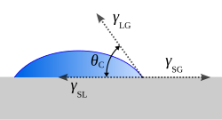
The adhesion characteristics can be observed and tested with a goniometer test. The surface energy characteristics of the silicon wafer can be measured by placing a drop of deionized water or ethylene glycol and measuring the contact angle of the droplet. Using the Young's relation and tabulated values for interfacial energy, we can estimate the surface energy of the solid. [8]

•Young's Relation:

 - Interfacial energy between solid and vapor  - Interfacial energy between solid and liquid  - Interfacial energy between liquid and vapor θ   - Contact Angle
Schematic of a drop of liquid on a solid surface, allowing for further explanation of the Young's Relation equation. Contact angle.svg
Schematic of a drop of liquid on a solid surface, allowing for further explanation of the Young's Relation equation.

Positive resist

Positive photoresists are composed of a novolac resin, ethyl lactate solvent, and Diazonaphthaquinone (DQ) as the photoactive compound. [9] Positive photoresist reacts with light to cause the polymer to break down and become soluble in a developer solution. Positive resist has better resistance to etchant than negative photoresist. Positive resists are better for producing small feature size, but does not adhere to silicon wafers as well as negative resist. When making small features it is critical to have good adhesion.

Negative resist

Negative photoresists are composed of a poly(cis-isoprene) matrix, xylene solvent, and bis-arylazide as the photoactive compound. Negative photoresists react to light by polymerizing. The unexposed portions can be removed by using a developer solution. negative resist has better adhesion and is great for features greater than 2 μm in size.

HMDS

Treating a silicon wafer with HMDS, to make the silicon wafer hydrophobic. Surface Chemistry of HMDS.jpg
Treating a silicon wafer with HMDS, to make the silicon wafer hydrophobic.

A common method to increase adhesion of photoresist on the silicon wafer surface is to treat the wafer with Hexamethyldisilazane (HMDS). A new silicon wafer has a polar surface and has some adsorbed water on the surface. [10] The wafer can undergo a dehydration bake to remove adsorbed water, and followed by the HMDS treatment also known as the priming stage. HMDS can be dispensed in liquid form onto the wafer using a syringe while the wafer is attached to a vacuum chuck in a spin coater. HMDS can also be applied in gas form in the process known as the vapor prime. The HMDS promotes good photoresist-to-wafer adhesion because it ensures the wafer surface is hydrophobic. After HMDS treatment the silicon surface oxide becomes silated, leaving a non-polar surface. [11] The pristine silicon (100) face has a surface energy value of 56.9 mN/m, which is reduced to a value of 44.1 mN/m after HMDS treatment [12] The molecular formula for hexamethyldisilazane is C6H19NSi2.

The chemical composition of hexamethylsilazane Hexamethylsilazane.svg
The chemical composition of hexamethylsilazane
3D image of HMDS HMDS-3D.png
3D image of HMDS

Spin coating

There are four basic parameters that are involved in spin coating: solution viscosity, solid content (density), angular speed, and spin time. [13] A range of thicknesses can be achieved by spin coating. Most commonly the thicknesses range from 1-200 μm. The main properties that affect the thickness of the film are viscosity and spin speed. The more viscous the solvent the thicker the film will be and the faster the wafer is spun the thinner the film will be. By manipulating these two factors the different range of thicknesses is possible.

• thickness:

ρ - density μ - viscosity ω - angular velocity t - time 

The density and viscosity both relate to the actual properties of the photoresist. This parameter can be manipulated by diluting the photoresist and adding different components to it to change its properties. The angular velocity and time relate to the spin coater and how fast it is spinning and for how long.

A common issue in spin coating is a "beading" up of solvent at the edge of the silicon wafer. A process known as backside washing is most commonly used to spin this bead off of the wafer. By programming multiple different spin speeds into the spin coating apparatus the thickness of the solvent can be made uniform without the "beading" up at the edges.

A typical spin coating apparatus for applying HMDS and photoresist onto a silicon wafer Spinner.jpg
A typical spin coating apparatus for applying HMDS and photoresist onto a silicon wafer

Spin coating has its limitations, though. Currently engineers and scientist are working on figuring out a better way to apply photoresist to the substrate of a silicon wafer. Spin coating can result in issues with wafer topography such as non-round substrates, oversized substrates, fragile substrates and material consumption. One potential solution to this issue is spraying the photoresist onto the surface. [14] By spraying the photoresist onto the surface of the wafer as opposed to spin coating the photoresist, a lot of photoresist is saved, and smaller and more precise parts can be made. Spray coating is still in its development phase and much more research needs to be done to make it cost effective and applicable.

See also

Related Research Articles

<span class="mw-page-title-main">MEMS</span> Very small devices that incorporate moving components

MEMS is the technology of microscopic devices incorporating both electronic and moving parts. MEMS are made up of components between 1 and 100 micrometres in size, and MEMS devices generally range in size from 20 micrometres to a millimetre, although components arranged in arrays can be more than 1000 mm2. They usually consist of a central unit that processes data and several components that interact with the surroundings.

In integrated circuit manufacturing, photolithography or optical lithography is a general term used for techniques that use light to produce minutely patterned thin films of suitable materials over a substrate, such as a silicon wafer, to protect selected areas of it during subsequent etching, deposition, or implantation operations. Typically, ultraviolet light is used to transfer a geometric design from an optical mask to a light-sensitive chemical (photoresist) coated on the substrate. The photoresist either breaks down or hardens where it is exposed to light. The patterned film is then created by removing the softer parts of the coating with appropriate solvents, also known in this case as developers.

<span class="mw-page-title-main">Photoresist</span> Light-sensitive material used in making electronics

A photoresist is a light-sensitive material used in several processes, such as photolithography and photoengraving, to form a patterned coating on a surface. This process is crucial in the electronics industry.

<span class="mw-page-title-main">Surface energy</span> Excess energy at the surface of a material relative to its interior

In surface science, surface free energy quantifies the disruption of intermolecular bonds that occurs when a surface is created. In solid-state physics, surfaces must be intrinsically less energetically favorable than the bulk of the material, otherwise there would be a driving force for surfaces to be created, removing the bulk of the material. The surface energy may therefore be defined as the excess energy at the surface of a material compared to the bulk, or it is the work required to build an area of a particular surface. Another way to view the surface energy is to relate it to the work required to cut a bulk sample, creating two surfaces. There is "excess energy" as a result of the now-incomplete, unrealized bonding between the two created surfaces.

A thin film is a layer of material ranging from fractions of a nanometer (monolayer) to several micrometers in thickness. The controlled synthesis of materials as thin films is a fundamental step in many applications. A familiar example is the household mirror, which typically has a thin metal coating on the back of a sheet of glass to form a reflective interface. The process of silvering was once commonly used to produce mirrors, while more recently the metal layer is deposited using techniques such as sputtering. Advances in thin film deposition techniques during the 20th century have enabled a wide range of technological breakthroughs in areas such as magnetic recording media, electronic semiconductor devices, integrated passive devices, LEDs, optical coatings, hard coatings on cutting tools, and for both energy generation and storage. It is also being applied to pharmaceuticals, via thin-film drug delivery. A stack of thin films is called a multilayer.

Dry etching refers to the removal of material, typically a masked pattern of semiconductor material, by exposing the material to a bombardment of ions that dislodge portions of the material from the exposed surface. A common type of dry etching is reactive-ion etching. Unlike with many of the wet chemical etchants used in wet etching, the dry etching process typically etches directionally or anisotropically.

<span class="mw-page-title-main">Marangoni effect</span> Physical phenomenon between two fluids

The Marangoni effect is the mass transfer along an interface between two phases due to a gradient of the surface tension. In the case of temperature dependence, this phenomenon may be called thermo-capillary convection.

<span class="mw-page-title-main">Contact angle</span> The angle between a liquid–vapor interface and a solid surface

The contact angle is the angle, conventionally measured through the liquid, where a liquid–vapor interface meets a solid surface. It quantifies the wettability of a solid surface by a liquid via the Young equation. A given system of solid, liquid, and vapor at a given temperature and pressure has a unique equilibrium contact angle. However, in practice a dynamic phenomenon of contact angle hysteresis is often observed, ranging from the advancing (maximal) contact angle to the receding (minimal) contact angle. The equilibrium contact is within those values, and can be calculated from them. The equilibrium contact angle reflects the relative strength of the liquid, solid, and vapour molecular interaction.

<span class="mw-page-title-main">Stepper</span> Photolithographic Tool

A stepper is a device used in the manufacture of integrated circuits (ICs) that is similar in operation to a slide projector or a photographic enlarger. Stepper is short for step-and-repeat camera. Steppers are an essential part of the complex process, called photolithography, which creates millions of microscopic circuit elements on the surface of silicon wafers out of which chips are made. These chips form the heart of ICs such as computer processors, memory chips, and many other devices.

<span class="mw-page-title-main">Spin coating</span>

Spin coating is a procedure used to deposit uniform thin films onto flat substrates. Usually a small amount of coating material is applied on the center of the substrate, which is either spinning at low speed or not spinning at all. The substrate is then rotated at speeds up to 10,000 rpm to spread the coating material by centrifugal force. A machine used for spin coating is called a spin coater, or simply spinner.

<span class="mw-page-title-main">SU-8 photoresist</span> Epoxy-based polymer

SU-8 is a commonly used epoxy-based negative photoresist. Negative refers to a photoresist whereby the parts exposed to UV become cross-linked, while the remainder of the film remains soluble and can be washed away during development.

<span class="mw-page-title-main">Etching (microfabrication)</span> Technique in microfabrication used to remove material and create structures

Etching is used in microfabrication to chemically remove layers from the surface of a wafer during manufacturing. Etching is a critically important process module, and every wafer undergoes many etching steps before it is complete.

Microlithography is a general name for any manufacturing process that can create a minutely patterned thin film of protective materials over a substrate, such as a silicon wafer, in order to protect selected areas of it during subsequent etching, deposition, or implantation operations. The term is normally used for processes that can reliably produce features of microscopic size, such as 10 micrometres or less. The term nanolithography may be used to designate processes that can produce nanoscale features, such as less than 100 nanometres.

Adhesive bonding describes a wafer bonding technique with applying an intermediate layer to connect substrates of different types of materials. Those connections produced can be soluble or insoluble. The commercially available adhesive can be organic or inorganic and is deposited on one or both substrate surfaces. Adhesives, especially the well-established SU-8, and benzocyclobutene (BCB), are specialized for MEMS or electronic component production.

<span class="mw-page-title-main">Ultrasonic nozzle</span>

Ultrasonic nozzles are a type of spray nozzle that use high frequency vibrations produced by piezoelectric transducers acting upon the nozzle tip that create capillary waves in a liquid film. Once the amplitude of the capillary waves reaches a critical height, they become too tall to support themselves and tiny droplets fall off the tip of each wave resulting in atomization.

Glass frit bonding, also referred to as glass soldering or seal glass bonding, describes a wafer bonding technique with an intermediate glass layer. It is a widely used encapsulation technology for surface micro-machined structures, e.g., accelerometers or gyroscopes. This technique utilizes low melting-point glass and therefore provides various advantages including that viscosity of glass decreases with an increase of temperature. The viscous flow of glass has effects to compensate and planarize surface irregularities, convenient for bonding wafers with a high roughness due to plasma etching or deposition. A low viscosity promotes hermetically sealed encapsulation of structures based on a better adaption of the structured shapes. Further, the coefficient of thermal expansion (CTE) of the glass material is adapted to silicon. This results in low stress in the bonded wafer pair. The glass has to flow and wet the soldered surfaces well below the temperature where deformation or degradation of either of the joined materials or nearby structures occurs. The usual temperature of achieving flowing and wetting is between 450 and 550 °C.

Adsorption is the adhesion of ions or molecules onto the surface of another phase. Adsorption may occur via physisorption and chemisorption. Ions and molecules can adsorb to many types of surfaces including polymer surfaces. A polymer is a large molecule composed of repeating subunits bound together by covalent bonds. In dilute solution, polymers form globule structures. When a polymer adsorbs to a surface that it interacts favorably with, the globule is essentially squashed, and the polymer has a pancake structure.

The surface chemistry of paper is responsible for many important paper properties, such as gloss, waterproofing, and printability. Many components are used in the paper-making process that affect the surface.

Three-dimensional (3D) microfabrication refers to manufacturing techniques that involve the layering of materials to produce a three-dimensional structure at a microscopic scale. These structures are usually on the scale of micrometers and are popular in microelectronics and microelectromechanical systems.

Glossary of microelectronics manufacturing terms

References

  1. Fourkas, John T. (15 April 2010). "Nanoscale Photolithography with Visible Light". The Journal of Physical Chemistry Letters. 1 (8): 1221–1227. doi:10.1021/jz1002082.
  2. Microelectromechanical systems
  3. Xiaoge, Gregory Zhang (2001-09-30). Silicon/Electrolyte Interface. ISBN   9780306465413.
  4. Xiaoge, Gregory Zhang (2001-09-30). Silicon/Electrolyte Interface. ISBN   9780306465413.
  5. Xiaoge, Gregory Zhang (2001-09-30). Silicon/Electrolyte Interface. ISBN   9780306465413.
  6. Jaccodine, R J (1963). "Surface Energy of Germanium and Silicon". Journal of the Electrochemical Society. 110 (6): 524. Bibcode:1963JElS..110..524J. doi:10.1149/1.2425806 . Retrieved 3 June 2012.
  7. Zdyb, A; Olchowik, Mucha (2006). "Dependence of GaAs and Si surface energy on the misorientation angle of crystal planes". Materials Science - Poland. 24 (4): 1110.
  8. Chow, T S (13 July 1998). "Wetting of rough surfaces". Journal of Physics: Condensed Matter. 10 (27): L445–L451. Bibcode:1998JPCM...10L.445C. doi:10.1088/0953-8984/10/27/001. S2CID   250874015.
  9. Darling, R. B. "Positive Photoresists" (PDF). University of Washington. Archived from the original (PDF) on 15 August 2010. Retrieved 3 June 2012.
  10. "Substrate Cleaning Adhesion Promotion" (PDF). Retrieved 24 May 2012.
  11. Chen, Jem-Kun; Hsieh, Huang; Kuo, Chang (29 October 2008). "Poly (methyl methacralate) Brushes" (PDF). Macromolecules. 41 (22): 8729. Bibcode:2008MaMol..41.8729C. doi:10.1021/ma801127m.[ permanent dead link ]
  12. Chen, Hsieh, Huang, Li, Kuo, Chang, Jem-Kun, Chih-Yi, Chih-Feng, P.M., Shiao-Wei, Feng-Chih. "Using Solvent Immersion to Fabricate Variably Patterned Poly(methyl methacrylate) Brushes on Silicon Surfaces" (PDF). Macromolecules, 2008, 41 (22).{{cite web}}: CS1 maint: multiple names: authors list (link)[ permanent dead link ]
  13. Shie, Jie-Ren; Yang, Yung-Kuand (26 April 2008). "Optimization of a photoresist coating process for photolithography in wafer manufacture via a radial basis neural network: A case study". Microelectronic Engineering. 85 (7): 1664–1670. doi:10.1016/j.mee.2008.04.019.
  14. Pabo, E.F. (7–9 December 2011). "Advances in spray coating technologies for MEMS, 3DICs and additional applications". 2011 IEEE 13th Electronics Packaging Technology Conference. Electronics Packaging Technology Conference. Vol. 13. pp. 349–353. doi:10.1109/EPTC.2011.6184444. ISBN   978-1-4577-1982-0. S2CID   34003957.