Related Research Articles
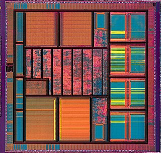
Very large-scale integration (VLSI) is the process of creating an integrated circuit (IC) by combining millions of MOS transistors onto a single chip. VLSI began in the 1970s when MOS integrated circuit chips were widely adopted, enabling complex semiconductor and telecommunication technologies to be developed. The microprocessor and memory chips are VLSI devices. Before the introduction of VLSI technology, most ICs had a limited set of functions they could perform. An electronic circuit might consist of a CPU, ROM, RAM and other glue logic. VLSI enables IC designers to add all of these into one chip.
In computer engineering, a hardware description language (HDL) is a specialized computer language used to describe the structure and behavior of electronic circuits, and most commonly, digital logic circuits.

An application-specific integrated circuit is an integrated circuit (IC) chip customized for a particular use, rather than intended for general-purpose use. For example, a chip designed to run in a digital voice recorder or a high-efficiency video codec is an ASIC. Application-specific standard product (ASSP) chips are intermediate between ASICs and industry standard integrated circuits like the 7400 series or the 4000 series. ASIC chips are typically fabricated using metal-oxide-semiconductor (MOS) technology, as MOS integrated circuit chips.
Electronic design automation (EDA), also referred to as electronic computer-aided design (ECAD), is a category of software tools for designing electronic systems such as integrated circuits and printed circuit boards. The tools work together in a design flow that chip designers use to design and analyze entire semiconductor chips. Since a modern semiconductor chip can have billions of components, EDA tools are essential for their design; this article in particular describes EDA specifically with respect to integrated circuits (ICs).

Integrated circuit layout, also known IC layout, IC mask layout, or mask design, is the representation of an integrated circuit in terms of planar geometric shapes which correspond to the patterns of metal, oxide, or semiconductor layers that make up the components of the integrated circuit. Originally the overall process was called tapeout as historically early ICs used graphical black crepe tape on mylar media for photo imaging.
Silvaco Inc. develops and markets electronic design automation (EDA) and technology CAD (TCAD) software and semiconductor design IP (SIP). The company is headquartered in Santa Clara, California, and has a global presence with offices located in North America, Europe, and throughout Asia. Since its founding in 1984, Silvaco has grown to become a large privately held EDA company. The company has been known by at least two other names: Silvaco International, and Silvaco Data Systems.
Formal equivalence checking process is a part of electronic design automation (EDA), commonly used during the development of digital integrated circuits, to formally prove that two representations of a circuit design exhibit exactly the same behavior.
Place and route is a stage in the design of printed circuit boards, integrated circuits, and field-programmable gate arrays. As implied by the name, it is composed of two steps, placement and routing. The first step, placement, involves deciding where to place all electronic components, circuitry, and logic elements in a generally limited amount of space. This is followed by routing, which decides the exact design of all the wires needed to connect the placed components. This step must implement all the desired connections while following the rules and limitations of the manufacturing process.
In semiconductor design, standard cell methodology is a method of designing application-specific integrated circuits (ASICs) with mostly digital-logic features. Standard cell methodology is an example of design abstraction, whereby a low-level very-large-scale integration (VLSI) layout is encapsulated into an abstract logic representation.
Static timing analysis (STA) is a simulation method of computing the expected timing of a synchronous digital circuit without requiring a simulation of the full circuit.

OrCAD Systems Corporation was a software company that made OrCAD, a proprietary software tool suite used primarily for electronic design automation (EDA). The software is used mainly by electronic design engineers and electronic technicians to create electronic schematics, perform mixed-signal simulation and electronic prints for manufacturing printed circuit boards. OrCAD was taken over by Cadence Design Systems in 1999 and was integrated with Cadence Allegro since 2005.
Integrated circuit design, or IC design, is a sub-field of electronics engineering, encompassing the particular logic and circuit design techniques required to design integrated circuits, or ICs. ICs consist of miniaturized electronic components built into an electrical network on a monolithic semiconductor substrate by photolithography.

Signal integrity or SI is a set of measures of the quality of an electrical signal. In digital electronics, a stream of binary values is represented by a voltage waveform. However, digital signals are fundamentally analog in nature, and all signals are subject to effects such as noise, distortion, and loss. Over short distances and at low bit rates, a simple conductor can transmit this with sufficient fidelity. At high bit rates and over longer distances or through various mediums, various effects can degrade the electrical signal to the point where errors occur and the system or device fails. Signal integrity engineering is the task of analyzing and mitigating these effects. It is an important activity at all levels of electronics packaging and assembly, from internal connections of an integrated circuit (IC), through the package, the printed circuit board (PCB), the backplane, and inter-system connections. While there are some common themes at these various levels, there are also practical considerations, in particular the interconnect flight time versus the bit period, that cause substantial differences in the approach to signal integrity for on-chip connections versus chip-to-chip connections.
An EDA database is a database specialized for the purpose of electronic design automation. These application specific databases are required because general purpose databases have historically not provided enough performance for EDA applications.
The Layout Versus Schematic (LVS) is the class of electronic design automation (EDA) verification software that determines whether a particular integrated circuit layout corresponds to the original schematic or circuit diagram of the design.

Technology computer-aided design is a branch of electronic design automation that models semiconductor fabrication and semiconductor device operation. The modeling of the fabrication is termed Process TCAD, while the modeling of the device operation is termed Device TCAD. Included are the modelling of process steps, and modelling of the behavior of the electrical devices based on fundamental physics, such as the doping profiles of the devices. TCAD may also include the creation of compact models, which try to capture the electrical behavior of such devices but do not generally derive them from the underlying physics. SPICE simulator itself is usually considered as part of ECAD rather than TCAD.
Electromagnetic field solvers are specialized programs that solve Maxwell's equations directly. They form a part of the field of electronic design automation, or EDA, and are commonly used in the design of integrated circuits and printed circuit boards. They are used when a solution from first principles is needed, or the highest accuracy is required.

In the design of integrated circuits, power network design is the analysis and design of on-chip conductor networks that distribute electrical power on a chip. As in all engineering, this involves tradeoffs - the network must have adequate performance, be sufficiently reliable, but should not use more resources than required.

In integrated circuit design, physical design is a step in the standard design cycle which follows after the circuit design. At this step, circuit representations of the components of the design are converted into geometric representations of shapes which, when manufactured in the corresponding layers of materials, will ensure the required functioning of the components. This geometric representation is called integrated circuit layout. This step is usually split into several sub-steps, which include both design and verification and validation of the layout.
In electronic design automation, parasitic extraction is the calculation of the parasitic effects in both the designed devices and the required wiring interconnects of an electronic circuit: parasitic capacitances, parasitic resistances and parasitic inductances, commonly called parasitic devices, parasitic components, or simply parasitics.
References
Electronic Design Automation For Integrated Circuits Handbook, by Lavagno, Martin and Scheffer, ( ISBN 0-8493-3096-3 ) A survey of the field of electronic design automation. This summary was derived, with permission, from Volume II, Chapter 22, Layout Extraction, by William Kao, Chi-Yuan Lo, Mark Basel, Raminderpal Singh, Peter Spink, and Lou Scheffer.