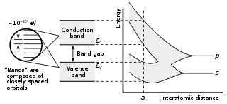
In solid-state physics and solid-state chemistry, a band gap, also called a bandgap or energy gap, is an energy range in a solid where no electronic states exist. In graphs of the electronic band structure of solids, the band gap refers to the energy difference between the top of the valence band and the bottom of the conduction band in insulators and semiconductors. It is the energy required to promote an electron from the valence band to the conduction band. The resulting conduction-band electron are free to move within the crystal lattice and serve as charge carriers to conduct electric current. It is closely related to the HOMO/LUMO gap in chemistry. If the valence band is completely full and the conduction band is completely empty, then electrons cannot move within the solid because there are no available states. If the electrons are not free to move within the crystal lattice, then there is no generated current due to no net charge carrier mobility. However, if some electrons transfer from the valence band to the conduction band, then current can flow. Therefore, the band gap is a major factor determining the electrical conductivity of a solid. Substances having large band gaps are generally insulators, those with small band gaps are semiconductor, and conductors either have very small band gaps or none, because the valence and conduction bands overlap to form a continuous band.

A laser diode is a semiconductor device similar to a light-emitting diode in which a diode pumped directly with electrical current can create lasing conditions at the diode's junction.

Gallium arsenide (GaAs) is a III-V direct band gap semiconductor with a zinc blende crystal structure.

Photonics is a branch of optics that involves the application of generation, detection, and manipulation of light in the form of photons through emission, transmission, modulation, signal processing, switching, amplification, and sensing. Photonics is closely related to quantum electronics, where quantum electronics deals with the theoretical part of it while photonics deal with its engineering applications. Though covering all light's technical applications over the whole spectrum, most photonic applications are in the range of visible and near-infrared light. The term photonics developed as an outgrowth of the first practical semiconductor light emitters invented in the early 1960s and optical fibers developed in the 1970s.

A quantum well is a potential well with only discrete energy values.
Silvaco Group, Inc., develops and markets electronic design automation (EDA) and technology CAD (TCAD) software and semiconductor design IP (SIP). The company is headquartered in Santa Clara, California, and has offices in North America, Europe, and throughout Asia. Founded in 1984, Silvaco is a publicly traded EDA company. The company has been known by at least two other names: Silvaco International, and Silvaco Data Systems.
Indium gallium nitride is a semiconductor material made of a mix of gallium nitride (GaN) and indium nitride (InN). It is a ternary group III/group V direct bandgap semiconductor. Its bandgap can be tuned by varying the amount of indium in the alloy. InxGa1−xN has a direct bandgap span from the infrared for InN to the ultraviolet of GaN. The ratio of In/Ga is usually between 0.02/0.98 and 0.3/0.7.

Zinc telluride is a binary chemical compound with the formula ZnTe. This solid is a semiconductor material with a direct band gap of 2.26 eV. It is usually a p-type semiconductor. Its crystal structure is cubic, like that for sphalerite and diamond.
Aluminium gallium indium phosphide is a semiconductor material that provides a platform for the development of multi-junction photovoltaics and optoelectronic devices. It has a direct bandgap ranging from ultraviolet to infrared photon energies.

Technology computer-aided design is a branch of electronic design automation (EDA) that models semiconductor fabrication and semiconductor device operation. The modeling of the fabrication is termed process TCAD, while the modeling of the device operation is termed device TCAD. Included are the modelling of process steps, and modelling of the behavior of the electrical devices based on fundamental physics, such as the doping profiles of the devices. TCAD may also include the creation of "compact models", which try to capture the electrical behavior of such devices but do not generally derive them from the underlying physics. SPICE simulator itself is usually considered as part of EDA rather than TCAD.

Semiconductor process simulation is the modeling of the fabrication of semiconductor devices such as transistors. It is a branch of electronic design automation, and part of a sub-field known as technology CAD, or TCAD.
Semiconductor device modeling creates models for the behavior of the electrical devices based on fundamental physics, such as the doping profiles of the devices. It may also include the creation of compact models, which try to capture the electrical behavior of such devices but do not generally derive them from the underlying physics. Normally it starts from the output of a semiconductor process simulation.
A photonic integrated circuit (PIC) or integrated optical circuit is a microchip containing two or more photonic components that form a functioning circuit. This technology detects, generates, transports, and processes light. Photonic integrated circuits use photons as opposed to electrons that are used by electronic integrated circuits. The major difference between the two is that a photonic integrated circuit provides functions for information signals imposed on optical wavelengths typically in the visible spectrum or near-infrared (850–1650 nm).
A resonant-tunneling diode (RTD) is a diode with a resonant-tunneling structure in which electrons can tunnel through some resonant states at certain energy levels. The current–voltage characteristic often exhibits negative differential resistance regions.

The Ferdinand-Braun-Institut, Leibniz-Institut für Höchstfrequenztechnik (FBH) is a research institute, which is a member of the Gottfried Wilhelm Leibniz Scientific Community. The institute is located in Berlin at the Wissenschafts- und Wirtschaftsstandort Adlershof (WISTA), its research activity is applied science in the fields of III-V electronics, photonics, integrated quantum technology and III-V technology
Archimedes is a TCAD package for use by engineers to design and simulate submicron and mesoscopic semiconductor devices. Archimedes is free software and thus it can be copied, modified and redistributed under GPL. Archimedes uses the Ensemble Monte Carlo method and is able to simulate physics effects and transport for electrons and heavy holes in Silicon, Germanium, GaAs, InSb, AlSb, AlAs, AlxInxSb, AlxIn(1-x)Sb, AlP, AlSb, GaP, GaSb, InP and their compounds, along with Silicon Oxide. Applied and/or self-consistent electrostatic and magnetic fields are handled with the Poisson and Faraday equations.
Roger John Malik is a physicist, engineer and inventor.
James J. Coleman is an electrical engineer who worked at Bell Labs, Rockwell International, and the University of Illinois, Urbana. He is best known for his work on semiconductor lasers, materials and devices including strained-layer indium gallium arsenide lasers and selective area epitaxy. Coleman is a Fellow of the IEEE and a member of the US National Academy of Engineering.
Robert W. Dutton is an American electrical engineer. At Stanford University, he is the Robert and Barbara Kleist Professor of Electrical Engineering, Emeritus. Dutton also served as the undergraduate advisor for Stanford University Department of Electrical Engineering, succeeded by John M. Pauly.