The Hall effect is the production of a potential difference across an electrical conductor that is transverse to an electric current in the conductor and to an applied magnetic field perpendicular to the current. It was discovered by Edwin Hall in 1879.
Magnetoresistance is the tendency of a material to change the value of its electrical resistance in an externally-applied magnetic field. There are a variety of effects that can be called magnetoresistance. Some occur in bulk non-magnetic metals and semiconductors, such as geometrical magnetoresistance, Shubnikov–de Haas oscillations, or the common positive magnetoresistance in metals. Other effects occur in magnetic metals, such as negative magnetoresistance in ferromagnets or anisotropic magnetoresistance (AMR). Finally, in multicomponent or multilayer systems, giant magnetoresistance (GMR), tunnel magnetoresistance (TMR), colossal magnetoresistance (CMR), and extraordinary magnetoresistance (EMR) can be observed.
In solid state physics, a particle's effective mass is the mass that it seems to have when responding to forces, or the mass that it seems to have when interacting with other identical particles in a thermal distribution. One of the results from the band theory of solids is that the movement of particles in a periodic potential, over long distances larger than the lattice spacing, can be very different from their motion in a vacuum. The effective mass is a quantity that is used to simplify band structures by modeling the behavior of a free particle with that mass. For some purposes and some materials, the effective mass can be considered to be a simple constant of a material. In general, however, the value of effective mass depends on the purpose for which it is used, and can vary depending on a number of factors.

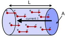
In physics, drift velocity is the average velocity attained by charged particles, such as electrons, in a material due to an electric field. In general, an electron in a conductor will propagate randomly at the Fermi velocity, resulting in an average velocity of zero. Applying an electric field adds to this random motion a small net flow in one direction; this is the drift.
Space charge is an interpretation of a collection of electric charges in which excess electric charge is treated as a continuum of charge distributed over a region of space rather than distinct point-like charges. This model typically applies when charge carriers have been emitted from some region of a solid—the cloud of emitted carriers can form a space charge region if they are sufficiently spread out, or the charged atoms or molecules left behind in the solid can form a space charge region.
The van der Pauw Method is a technique commonly used to measure the resistivity and the Hall coefficient of a sample. Its strength lies in its ability to accurately measure the properties of a sample of any arbitrary shape, as long as the sample is approximately two-dimensional, solid, and the electrodes are placed on its perimeter. The van der Pauw method employs a four-point probe placed around the perimeter of the sample, in contrast to the linear four point probe: this allows the van der Pauw method to provide an average resistivity of the sample, whereas a linear array provides the resistivity in the sensing direction. This difference becomes important for anisotropic materials, which can be properly measured using the Montgomery Method, an extension of the van der Pauw Method.
A continuity equation or transport equation is an equation that describes the transport of some quantity. It is particularly simple and powerful when applied to a conserved quantity, but it can be generalized to apply to any extensive quantity. Since mass, energy, momentum, electric charge and other natural quantities are conserved under their respective appropriate conditions, a variety of physical phenomena may be described using continuity equations.

A p–n junction is a combination of two types of semiconductor materials, p-type and n-type, in a single crystal. The "n" (negative) side contains freely-moving electrons, while the "p" (positive) side contains freely-moving electron holes. Connecting the two materials causes creation of a depletion region near the boundary, as the free electrons fill the available holes, which in turn allows electric current to pass through the junction only in one direction.
In solid-state physics, the electron mobility characterises how quickly an electron can move through a metal or semiconductor when pushed or pulled by an electric field. There is an analogous quantity for holes, called hole mobility. The term carrier mobility refers in general to both electron and hole mobility.

The Seebeck coefficient of a material is a measure of the magnitude of an induced thermoelectric voltage in response to a temperature difference across that material, as induced by the Seebeck effect. The SI unit of the Seebeck coefficient is volts per kelvin (V/K), although it is more often given in microvolts per kelvin (μV/K).
Electrical mobility is the ability of charged particles to move through a medium in response to an electric field that is pulling them. The separation of ions according to their mobility in gas phase is called ion mobility spectrometry, in liquid phase it is called electrophoresis.
In semiconductor physics, the depletion region, also called depletion layer, depletion zone, junction region, space charge region, or space charge layer, is an insulating region within a conductive, doped semiconductor material where the mobile charge carriers have diffused away, or forced away by an electric field. The only elements left in the depletion region are ionized donor or acceptor impurities. This region of uncovered positive and negative ions is called the depletion region due to the depletion of carriers in this region, leaving none to carry a current. Understanding the depletion region is key to explaining modern semiconductor electronics: diodes, bipolar junction transistors, field-effect transistors, and variable capacitance diodes all rely on depletion region phenomena.
In physics, the Einstein relation is a previously unexpected connection revealed independently by William Sutherland in 1904, Albert Einstein in 1905, and by Marian Smoluchowski in 1906 in their works on Brownian motion. The more general form of the equation in the classical case is
In semiconductor physics, the Haynes–Shockley experiment was an experiment that demonstrated that diffusion of minority carriers in a semiconductor could result in a current. The experiment was reported in a short paper by Haynes and Shockley in 1948, with a more detailed version published by Shockley, Pearson, and Haynes in 1949. The experiment can be used to measure carrier mobility, carrier lifetime, and diffusion coefficient.
The word electricity refers generally to the movement of electrons, or other charge carriers, through a conductor in the presence of a potential difference or an electric field. The speed of this flow has multiple meanings. In everyday electrical and electronic devices, the signals travel as electromagnetic waves typically at 50%–99% of the speed of light in vacuum. The electrons themselves move much more slowly. See drift velocity and electron mobility.
The convection–diffusion equation is a combination of the diffusion and convection (advection) equations, and describes physical phenomena where particles, energy, or other physical quantities are transferred inside a physical system due to two processes: diffusion and convection. Depending on context, the same equation can be called the advection–diffusion equation, drift–diffusion equation, or (generic) scalar transport equation.
Diffusion current is a current in a semiconductor caused by the diffusion of charge carriers. This is the current which is due to the transport of charges occurring because of non-uniform concentration of charged particles in a semiconductor. The drift current, by contrast, is due to the motion of charge carriers due to the force exerted on them by an electric field. Diffusion current can be in the same or opposite direction of a drift current. The diffusion current and drift current together are described by the drift–diffusion equation.

The theory of solar cells explains the process by which light energy in photons is converted into electric current when the photons strike a suitable semiconductor device. The theoretical studies are of practical use because they predict the fundamental limits of a solar cell, and give guidance on the phenomena that contribute to losses and solar cell efficiency.
A p–n diode is a type of semiconductor diode based upon the p–n junction. The diode conducts current in only one direction, and it is made by joining a p-type semiconducting layer to an n-type semiconducting layer. Semiconductor diodes have multiple uses including rectification of alternating current to direct current, in the detection of radio signals, and emitting and detecting light.
Charge transport mechanisms are theoretical models that aim to quantitatively describe the electric current flow through a given medium.


