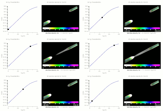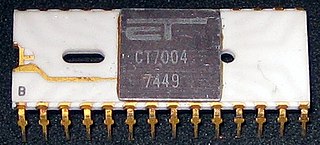
The metal–oxide–semiconductor field-effect transistor is a type of field-effect transistor (FET), most commonly fabricated by the controlled oxidation of silicon. It has an insulated gate, the voltage of which determines the conductivity of the device. This ability to change conductivity with the amount of applied voltage can be used for amplifying or switching electronic signals. The term metal–insulator–semiconductor field-effect transistor (MISFET) is almost synonymous with MOSFET. Another near-synonym is insulated-gate field-effect transistor (IGFET).

A radiation dosimeter is a device that measures dose uptake of external ionizing radiation. It is worn by the person being monitored when used as a personal dosimeter, and is a record of the radiation dose received. Modern electronic personal dosimeters can give a continuous readout of cumulative dose and current dose rate, and can warn the wearer with an audible alarm when a specified dose rate or a cumulative dose is exceeded. Other dosimeters, such as thermoluminescent or film types, require processing after use to reveal the cumulative dose received, and cannot give a current indication of dose while being worn.

An EPROM, or erasable programmable read-only memory, is a type of programmable read-only memory (PROM) chip that retains its data when its power supply is switched off. Computer memory that can retrieve stored data after a power supply has been turned off and back on is called non-volatile. It is an array of floating-gate transistors individually programmed by an electronic device that supplies higher voltages than those normally used in digital circuits. Once programmed, an EPROM can be erased by exposing it to strong ultraviolet (UV) light source. EPROMs are easily recognizable by the transparent fused quartz window on the top of the package, through which the silicon chip is visible, and which permits exposure to ultraviolet light during erasing.
Radiation dosimetry in the fields of health physics and radiation protection is the measurement, calculation and assessment of the ionizing radiation dose absorbed by an object, usually the human body. This applies both internally, due to ingested or inhaled radioactive substances, or externally due to irradiation by sources of radiation.
Radiation protection, also known as radiological protection, is defined by the International Atomic Energy Agency (IAEA) as "The protection of people from harmful effects of exposure to ionizing radiation, and the means for achieving this". Exposure can be from a source of radiation external to the human body or due to internal irradiation caused by the ingestion of radioactive contamination.
In semiconductor manufacturing, silicon on insulator (SOI) technology is fabrication of silicon semiconductor devices in a layered silicon–insulator–silicon substrate, to reduce parasitic capacitance within the device, thereby improving performance. SOI-based devices differ from conventional silicon-built devices in that the silicon junction is above an electrical insulator, typically silicon dioxide or sapphire. The choice of insulator depends largely on intended application, with sapphire being used for high-performance radio frequency (RF) and radiation-sensitive applications, and silicon dioxide for diminished short-channel effects in other microelectronics devices. The insulating layer and topmost silicon layer also vary widely with application.

The threshold voltage, commonly abbreviated as Vth or VGS(th), of a field-effect transistor (FET) is the minimum gate-to-source voltage (VGS) that is needed to create a conducting path between the source and drain terminals. It is an important scaling factor to maintain power efficiency.

A film badge dosimeter or film badge is a personal dosimeter used for monitoring cumulative radiation dose due to ionizing radiation.
In the semiconductor industry, the term high-κ dielectric refers to a material with a high dielectric constant, as compared to silicon dioxide. High-κ dielectrics are used in semiconductor manufacturing processes where they are usually used to replace a silicon dioxide gate dielectric or another dielectric layer of a device. The implementation of high-κ gate dielectrics is one of several strategies developed to allow further miniaturization of microelectronic components, colloquially referred to as extending Moore's Law. Sometimes these materials are called "high-k", instead of "high-κ".
Capacitance–voltage profiling is a technique for characterizing semiconductor materials and devices. The applied voltage is varied, and the capacitance is measured and plotted as a function of voltage. The technique uses a metal–semiconductor junction or a p–n junction or a MOSFET to create a depletion region, a region which is empty of conducting electrons and holes, but may contain ionized donors and electrically active defects or traps. The depletion region with its ionized charges inside behaves like a capacitor. By varying the voltage applied to the junction it is possible to vary the depletion width. The dependence of the depletion width upon the applied voltage provides information on the semiconductor's internal characteristics, such as its doping profile and electrically active defect densities., Measurements may be done at DC, or using both DC and a small-signal AC signal, or using a large-signal transient voltage.
Charge trap flash (CTF) is a semiconductor memory technology used in creating non-volatile NOR and NAND flash memory. It is a type of floating-gate MOSFET memory technology, but differs from the conventional floating-gate technology in that it uses a silicon nitride film to store electrons rather than the doped polycrystalline silicon typical of a floating-gate structure. This approach allows memory manufacturers to reduce manufacturing costs five ways:
- Fewer process steps are required to form a charge storage node
- Smaller process geometries can be used
- Multiple bits can be stored on a single flash memory cell
- Improved reliability
- Higher yield since the charge trap is less susceptible to point defects in the tunnel oxide layer
Hot carrier injection (HCI) is a phenomenon in solid-state electronic devices where an electron or a “hole” gains sufficient kinetic energy to overcome a potential barrier necessary to break an interface state. The term "hot" refers to the effective temperature used to model carrier density, not to the overall temperature of the device. Since the charge carriers can become trapped in the gate dielectric of a MOS transistor, the switching characteristics of the transistor can be permanently changed. Hot-carrier injection is one of the mechanisms that adversely affects the reliability of semiconductors of solid-state devices.
In semiconductor electronics fabrication technology, a self-aligned gate is a transistor manufacturing approach whereby the gate electrode of a MOSFET is used as a mask for the doping of the source and drain regions. This technique ensures that the gate is naturally and precisely aligned to the edges of the source and drain.

PMOS or pMOS logic is a family of digital circuits based on p-channel, enhancement mode metal–oxide–semiconductor field-effect transistors (MOSFETs). In the late 1960s and early 1970s, PMOS logic was the dominant semiconductor technology for large-scale integrated circuits before being superseded by NMOS and CMOS devices.

A quartz fiber dosimeter, sometimes called a self indicating pocket dosimeter (SIPD) or self reading pocket dosimeter (SRPD) or quartz fibre electrometer (QFE), is a type of radiation dosimeter, a pen-like device that measures the cumulative dose of ionizing radiation received by the device, usually over one work period. It is clipped to a person's clothing, normally a breast pocket for whole body exposure, to measure the user's exposure to radiation.
For electronic semiconductor devices, a native transistor is a variety of the MOS field-effect transistor that is intermediate between enhancement and depletion modes. Most common is the n-channel native transistor.
Polysilicon depletion effect is the phenomenon in which unwanted variation of threshold voltage of the MOSFET devices using polysilicon as gate material is observed, leading to unpredicted behavior of the electronic circuit. Because of this variation High-k Dielectric Metal Gates (HKMG) were introduced to solve the issue.

The field-effect transistor (FET) is a type of transistor that uses an electric field to control the flow of current in a semiconductor. It comes in two types: junction FET (JFET) and metal-oxide-semiconductor FET (MOSFET). FETs have three terminals: source, gate, and drain. FETs control the flow of current by the application of a voltage to the gate, which in turn alters the conductivity between the drain and source.
A ferroelectric field-effect transistor is a type of field-effect transistor that includes a ferroelectric material sandwiched between the gate electrode and source-drain conduction region of the device. Permanent electrical field polarisation in the ferroelectric causes this type of device to retain the transistor's state in the absence of any electrical bias.


