Related Research Articles

Crystallographic defects are interruptions of regular patterns in crystalline solids. They are common because positions of atoms or molecules at repeating fixed distances determined by the unit cell parameters in crystals, which exhibit a periodic crystal structure, are usually imperfect.

Ion implantation is a low-temperature process by which ions of one element are accelerated into a solid target, thereby changing the physical, chemical, or electrical properties of the target. Ion implantation is used in semiconductor device fabrication and in metal finishing, as well as in materials science research. The ions can alter the elemental composition of the target if they stop and remain in the target. Ion implantation also causes chemical and physical changes when the ions impinge on the target at high energy. The crystal structure of the target can be damaged or even destroyed by the energetic collision cascades, and ions of sufficiently high energy can cause nuclear transmutation.

Semiconductor device fabrication is the process used to manufacture semiconductor devices, typically integrated circuit (IC) chips such as modern computer processors, microcontrollers, and memory chips such as NAND flash and DRAM that are present in everyday electrical and electronic devices. It is a multiple-step sequence of photolithographic and chemical processing steps during which electronic circuits are gradually created on a wafer made of pure semiconducting material. Silicon is almost always used, but various compound semiconductors are used for specialized applications.
A semiconductor material has an electrical conductivity value falling between that of a conductor, such as metallic copper, and an insulator, such as glass. Its resistivity falls as its temperature rises; metals behave in the opposite way. Its conducting properties may be altered in useful ways by introducing impurities ("doping") into the crystal structure. When two differently doped regions exist in the same crystal, a semiconductor junction is created. The behavior of charge carriers, which include electrons, ions, and electron holes, at these junctions is the basis of diodes, transistors, and most modern electronics. Some examples of semiconductors are silicon, germanium, gallium arsenide, and elements near the so-called "metalloid staircase" on the periodic table. After silicon, gallium arsenide is the second-most common semiconductor and is used in laser diodes, solar cells, microwave-frequency integrated circuits, and others. Silicon is a critical element for fabricating most electronic circuits.

A semiconductor device is an electronic component that relies on the electronic properties of a semiconductor material for its function. Its conductivity lies between conductors and insulators. Semiconductor devices have replaced vacuum tubes in most applications. They conduct electric current in the solid state, rather than as free electrons across a vacuum or as free electrons and ions through an ionized gas.

In electronics, a wafer is a thin slice of semiconductor, such as a crystalline silicon (c-Si), used for the fabrication of integrated circuits and, in photovoltaics, to manufacture solar cells. The wafer serves as the substrate for microelectronic devices built in and upon the wafer. It undergoes many microfabrication processes, such as doping, ion implantation, etching, thin-film deposition of various materials, and photolithographic patterning. Finally, the individual microcircuits are separated by wafer dicing and packaged as an integrated circuit.

Gallium arsenide (GaAs) is a III-V direct band gap semiconductor with a zinc blende crystal structure.

The Czochralski method, also Czochralski technique or Czochralski process, is a method of crystal growth used to obtain single crystals of semiconductors, metals, salts and synthetic gemstones. The method is named after Polish scientist Jan Czochralski, who invented the method in 1915 while investigating the crystallization rates of metals. He made this discovery by accident: instead of dipping his pen into his inkwell, he dipped it in molten tin, and drew a tin filament, which later proved to be a single crystal.

Silicon carbide (SiC), also known as carborundum, is a hard chemical compound containing silicon and carbon. A semiconductor, it occurs in nature as the extremely rare mineral moissanite, but has been mass-produced as a powder and crystal since 1893 for use as an abrasive. Grains of silicon carbide can be bonded together by sintering to form very hard ceramics that are widely used in applications requiring high endurance, such as car brakes, car clutches and ceramic plates in bulletproof vests. Large single crystals of silicon carbide can be grown by the Lely method and they can be cut into gems known as synthetic moissanite.
Epitaxy refers to a type of crystal growth or material deposition in which new crystalline layers are formed with one or more well-defined orientations with respect to the crystalline seed layer. The deposited crystalline film is called an epitaxial film or epitaxial layer. The relative orientation(s) of the epitaxial layer to the seed layer is defined in terms of the orientation of the crystal lattice of each material. For most epitaxial growths, the new layer is usually crystalline and each crystallographic domain of the overlayer must have a well-defined orientation relative to the substrate crystal structure. Epitaxy can involve single-crystal structures, although grain-to-grain epitaxy has been observed in granular films. For most technological applications, single domain epitaxy, which is the growth of an overlayer crystal with one well-defined orientation with respect to the substrate crystal, is preferred. Epitaxy can also play an important role while growing superlattice structures.
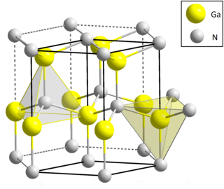
Gallium nitride is a binary III/V direct bandgap semiconductor commonly used in blue light-emitting diodes since the 1990s. The compound is a very hard material that has a Wurtzite crystal structure. Its wide band gap of 3.4 eV affords it special properties for applications in optoelectronic, high-power and high-frequency devices. For example, GaN is the substrate which makes violet (405 nm) laser diodes possible, without requiring nonlinear optical frequency-doubling.
In solid-state physics, the electron mobility characterises how quickly an electron can move through a metal or semiconductor when pulled by an electric field. There is an analogous quantity for holes, called hole mobility. The term carrier mobility refers in general to both electron and hole mobility.

In materials science, a dislocation or Taylor's dislocation is a linear crystallographic defect or irregularity within a crystal structure that contains an abrupt change in the arrangement of atoms. The movement of dislocations allow atoms to slide over each other at low stress levels and is known as glide or slip. The crystalline order is restored on either side of a glide dislocation but the atoms on one side have moved by one position. The crystalline order is not fully restored with a partial dislocation. A dislocation defines the boundary between slipped and unslipped regions of material and as a result, must either form a complete loop, intersect other dislocations or defects, or extend to the edges of the crystal. A dislocation can be characterised by the distance and direction of movement it causes to atoms which is defined by the Burgers vector. Plastic deformation of a material occurs by the creation and movement of many dislocations. The number and arrangement of dislocations influences many of the properties of materials.
In semiconductor production, doping is the intentional introduction of impurities into an intrinsic semiconductor for the purpose of modulating its electrical, optical and structural properties. The doped material is referred to as an extrinsic semiconductor.
In materials science, a single-crystal, or monocrystalline, solid is a material in which the crystal lattice of the entire sample is continuous and unbroken to the edges of the sample, with no grain boundaries. The absence of the defects associated with grain boundaries can give monocrystals unique properties, particularly mechanical, optical and electrical, which can also be anisotropic, depending on the type of crystallographic structure. These properties, in addition to making some gems precious, are industrially used in technological applications, especially in optics and electronics.
In the context of manufacturing integrated circuits, wafer dicing is the process by which die are separated from a wafer of semiconductor following the processing of the wafer. The dicing process can involve scribing and breaking, mechanical sawing or laser cutting. All methods are typically automated to ensure precision and accuracy. Following the dicing process the individual silicon chips are encapsulated into chip carriers which are then suitable for use in building electronic devices such as computers, etc.

An interstitial defect is a type of point crystallographic defect where an atom of the same or of a different type, occupies a normally unoccupied site in the crystal structure. When the atom is of the same type as those already present they are known as a self-interstitial defect. Alternatively, small atoms in some crystals may occupy interstitial sites, such as hydrogen in palladium. Interstitials can be produced by bombarding a crystal with elementary particles having energy above the displacement threshold for that crystal, but they may also exist in small concentrations in thermodynamic equilibrium. The presence of interstitial defects can modify the physical and chemical properties of a material.
A micropipe, also called a micropore, microtube, capillary defect or pinhole defect, is a crystallographic defect in a single crystal substrate. Minimizing the presence of micropipes is important in semiconductor manufacturing, as their presence on a wafer can result in the failure of integrated circuits made from that wafer.

The Wright etch is a preferential etch for revealing defects in <100>- and <111>-oriented, p- and n-type silicon wafers used for making transistors, microprocessors, memories, and other components. Revealing, identifying, and remedying such defects is essential for progress along the path predicted by Moore's Law. It was developed by Margaret Wright Jenkins (1936-2018) in 1976 while working in research and development at Motorola Inc. in Phoenix, AZ. It was published in 1977. This etchant reveals clearly defined oxidation-induced stacking faults, dislocations, swirls and striations with minimum surface roughness or extraneous pitting. These defects are known causes of shorts and current leakage in finished semiconductor devices should they fall across isolated junctions. A relatively low etch rate at room temperature provides etch control. The long shelf life of this etchant allows the solution to be stored in large quantities.
The Kyropoulos method, KY method, or Kyropoulos technique, is a method of bulk crystal growth used to obtain single crystals.
References
- ↑ Zhuang, D.; Edgar, J.H. (2005). "Wet etching of GaN, AlN, and SiC: a review". Materials Science and Engineering: R: Reports. 48 (1): 1–46. doi:10.1016/j.mser.2004.11.002. ISSN 0927-796X.
- ↑ Klaus Graff (8 March 2013). Metal Impurities in Silicon-Device Fabrication. Springer Science & Business Media. pp. 152–. ISBN 978-3-642-97593-6.
- ↑ J. Doneker; I. Rechenberg (1 January 1998). Defect Recognition and Image Processing in Semiconductors 1997: Proceedings of the seventh conference on Defect Recognition and Image Processing, Berlin, September 1997. CRC Press. pp. 248–. ISBN 978-0-7503-0500-6.
| | This standards- or measurement-related article is a stub. You can help Wikipedia by expanding it. |