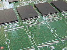
In microelectronics, a dual in-line package is an electronic component package with a rectangular housing and two parallel rows of electrical connecting pins. The package may be through-hole mounted to a printed circuit board (PCB) or inserted in a socket. The dual-inline format was invented by Don Forbes, Rex Rice and Bryant Rogers at Fairchild R&D in 1964, when the restricted number of leads available on circular transistor-style packages became a limitation in the use of integrated circuits. Increasingly complex circuits required more signal and power supply leads ; eventually microprocessors and similar complex devices required more leads than could be put on a DIP package, leading to development of higher-density chip carriers. Furthermore, square and rectangular packages made it easier to route printed-circuit traces beneath the packages.

A printed circuit board (PCB), also called printed wiring board (PWB), is a laminated sandwich structure of conductive and insulating layers, each with a pattern of traces, planes and other features etched from one or more sheet layers of copper laminated onto or between sheet layers of a non-conductive substrate. PCBs are used to connect or "wire" components to one another in an electronic circuit. Electrical components may be fixed to conductive pads on the outer layers, generally by soldering, which both electrically connects and mechanically fastens the components to the board. Another manufacturing process adds vias, metal-lined drilled holes that enable electrical interconnections between conductive layers, to boards with more than a single side.

Surface-mount technology (SMT), originally called planar mounting, is a method in which the electrical components are mounted directly onto the surface of a printed circuit board (PCB). An electrical component mounted in this manner is referred to as a surface-mount device (SMD). In industry, this approach has largely replaced the through-hole technology construction method of fitting components, in large part because SMT allows for increased manufacturing automation which reduces cost and improves quality. It also allows for more components to fit on a given area of substrate. Both technologies can be used on the same board, with the through-hole technology often used for components not suitable for surface mounting such as large transformers and heat-sinked power semiconductors.

Reflow soldering is a process in which a solder paste is used to temporarily attach anywhere from one to thousands of tiny electrical components to their contact pads, after which the entire assembly is subjected to controlled heat. The solder paste reflows in a molten state, creating permanent solder joints. Heating may be accomplished by passing the assembly through a reflow oven, under an infrared lamp, or by soldering individual joints with a hot air pencil.

In electronics, through-hole technology is a manufacturing scheme in which leads on the components are inserted through holes drilled in printed circuit boards (PCB) and soldered to pads on the opposite side, either by manual assembly or by the use of automated insertion mount machines.

TARGET 3001! is a CAD computer program for EDA and PCB design, developed by Ing.-Büro Friedrich in Germany. This software application has been available since 1992 and operates on Microsoft Windows. It supports the design of electronic schematics, PCBs, and device front panels. The software is available in English, German and French.

A via is an electrical connection between two or more metal layers of a printed circuit boards (PCB) or integrated circuit. Essentially a via is a small drilled hole that goes through two or more adjacent layers; the hole is plated with metal that forms an electrical connection through the insulating layers.

OrCAD Systems Corporation was a software company that made OrCAD, a proprietary software tool suite used primarily for electronic design automation (EDA). The software is used mainly by electronic design engineers and electronic technicians to create electronic schematics, and perform mixed-signal simulation and electronic prints for manufacturing printed circuit boards (PCBs). OrCAD was taken over by Cadence Design Systems in 1999 and was integrated with Cadence Allegro in 2005.

Solder paste is used in the manufacture of printed circuit boards to connect surface mount components to pads on the board. It is also possible to solder through-hole pin in paste components by printing solder paste in and over the holes. The sticky paste temporarily holds components in place; the board is then heated, melting the paste and forming a mechanical bond as well as an electrical connection. The paste is applied to the board by jet printing, stencil printing or syringe; then the components are put in place by a pick-and-place machine or by hand.

Flat no-leads packages such as quad-flat no-leads (QFN) and dual-flat no-leads (DFN) physically and electrically connect integrated circuits to printed circuit boards. Flat no-leads, also known as micro leadframe (MLF) and SON, is a surface-mount technology, one of several package technologies that connect ICs to the surfaces of PCBs without through-holes. Flat no-lead is a near chip scale plastic encapsulated package made with a planar copper lead frame substrate. Perimeter lands on the package bottom provide electrical connections to the PCB. Flat no-lead packages usually, but not always, include an exposed thermally conductive pad to improve heat transfer out of the IC. Heat transfer can be further facilitated by metal vias in the thermal pad. The QFN package is similar to the quad-flat package (QFP), and a ball grid array (BGA).

KiCad is a free software suite for electronic design automation (EDA). It facilitates the design and simulation of electronic hardware for PCB manufacturing. It features an integrated environment for schematic capture, PCB layout, manufacturing file viewing, ngspice-provided SPICE simulation, and engineering calculation. Tools exist within the package to create bill of materials, artwork, Gerber files, and 3D models of the PCB and its components.

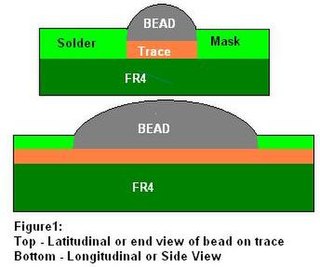
Bead probe technology (BPT) is technique used to provide electrical access to printed circuit board (PCB) circuitry for performing in-circuit testing (ICT). It makes use of small beads of solder placed onto the board's traces to allow measuring and controlling of the signals using a test probe. This permits test access to boards on which standard ICT test pads are not feasible due to space constraints.
Pad cratering is a mechanically induced fracture in the resin between copper foil and outermost layer of fiberglass of a printed circuit board (PCB). It may be within the resin or at the resin to fiberglass interface.

DipTrace is a proprietary software suite for electronic design automation (EDA) used for electronic schematic capture and printed circuit board layouts. DipTrace has four applications: schematic editor, PCB editor with built-in shape-based autorouter and 3D preview, component editor, and pattern editor.

In electronics, a chip carrier is one of several kinds of surface-mount technology packages for integrated circuits. Connections are made on all four edges of a square package; compared to the internal cavity for mounting the integrated circuit, the package overall size is large.

Pulsonix is an electronic design automation (EDA) software suite for schematic capture and PCB design. It is produced by WestDev, which is headquartered in Gloucestershire, England, with additional sales and distribution offices overseas. It was first released in 2001, and runs on Windows.
CircuitMaker is electronic design automation software for printed circuit board designs targeted at the hobby, hacker, and maker community. CircuitMaker is available as freeware, and the hardware designed with it may be used for commercial and non-commercial purposes without limitations. It is currently available publicly as version 2.0 by Altium Limited, with the first non-beta release on January 17, 2016.
Glossary of microelectronics manufacturing terms

Printed circuit board manufacturing is the process of manufacturing bare printed circuit boards (PCBs) and then populating them with electronic components. It involves the full assembly of a board into a functional circuit board.


