This article needs additional citations for verification .(April 2018) |
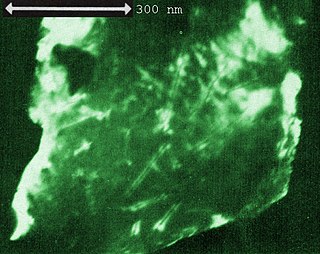
Ion implantation-induced nanoparticle formation is a technique for creating nanometer-sized particles for use in electronics.
This article needs additional citations for verification .(April 2018) |
Ion implantation-induced nanoparticle formation is a technique for creating nanometer-sized particles for use in electronics.
Ion Implantation is a technique extensively used in the field of materials science for material modification. The effect it has on nanomaterials allows manipulation of mechanical, electronic, morphological and optical properties. [1]
One-dimensional nano-materials are an important contributor to the creation of nano-devices i.e. field effect transistors, nanogenerators and solar cells. The offer the potential of high integration density, lower power consumption, higher speed and super high frequency.
The effects of ion implantation varies according to multiple variables. Collision cascade may occur during implantation and this causes of interstitials and vacancies in target materials (although these defects may be mitigated through dynamic annealing). Collision modes are nuclear collision, electron collision and charge exchange. Another process is the sputtering effect, which significantly affects the morphology and shape of nano-materials.

Ion implantation is a low-temperature process by which ions of one element are accelerated into a solid target, thereby changing the physical, chemical, or electrical properties of the target. Ion implantation is used in semiconductor device fabrication and in metal finishing, as well as in materials science research. The ions can alter the elemental composition of the target if they stop and remain in the target. Ion implantation also causes chemical and physical changes when the ions impinge on the target at high energy. The crystal structure of the target can be damaged or even destroyed by the energetic collision cascades, and ions of sufficiently high energy can cause nuclear transmutation.
Nanotechnology was defined by the National Nanotechnology Initiative as the manipulation of matter with at least one dimension sized from 1 to 100 nanometers (nm). At this scale, commonly known as the nanoscale, surface area and quantum mechanical effects become important in describing properties of matter. The definition of nanotechnology is inclusive of all types of research and technologies that deal with these special properties. It is therefore common to see the plural form "nanotechnologies" as well as "nanoscale technologies" to refer to the broad range of research and applications whose common trait is size. An earlier description of nanotechnology referred to the particular technological goal of precisely manipulating atoms and molecules for fabrication of macroscale products, also now referred to as molecular nanotechnology.
Nanosensors are nanoscale devices that measure physical quantities and convert these to signals that can be detected and analyzed. There are several ways proposed today to make nanosensors; these include top-down lithography, bottom-up assembly, and molecular self-assembly. There are different types of nanosensors in the market and in development for various applications, most notably in defense, environmental, and healthcare industries. These sensors share the same basic workflow: a selective binding of an analyte, signal generation from the interaction of the nanosensor with the bio-element, and processing of the signal into useful metrics.
Nanomaterials describe, in principle, materials of which a single unit is sized between 1 and 100 nm.
Irradiation is the process by which an object is exposed to radiation. An irradiator is a device used to expose an object to radiation, notably gamma radiation, for a variety of purposes. Irradiators may be used for sterilizing medical and pharmaceutical supplies, preserving foodstuffs, alteration of gemstone colors, studying radiation effects, eradicating insects through sterile male release programs, or calibrating thermoluminescent dosimeters (TLDs).

Focused ion beam, also known as FIB, is a technique used particularly in the semiconductor industry, materials science and increasingly in the biological field for site-specific analysis, deposition, and ablation of materials. A FIB setup is a scientific instrument that resembles a scanning electron microscope (SEM). However, while the SEM uses a focused beam of electrons to image the sample in the chamber, a FIB setup uses a focused beam of ions instead. FIB can also be incorporated in a system with both electron and ion beam columns, allowing the same feature to be investigated using either of the beams. FIB should not be confused with using a beam of focused ions for direct write lithography. These are generally quite different systems where the material is modified by other mechanisms.

Nanochemistry is an emerging sub-discipline of the chemical and material sciences that deals with the development of new methods for creating nanoscale materials. The term "nanochemistry" was first used by Ozin in 1992 as 'the uses of chemical synthesis to reproducibly afford nanomaterials from the atom "up", contrary to the nanoengineering and nanophysics approach that operates from the bulk "down"'. Nanochemistry focuses on solid-state chemistry that emphasizes synthesis of building blocks that are dependent on size, surface, shape, and defect properties, rather than the actual production of matter. Atomic and molecular properties mainly deal with the degrees of freedom of atoms in the periodic table. However, nanochemistry introduced other degrees of freedom that controls material's behaviors by transformation into solutions. Nanoscale objects exhibit novel material properties, largely as a consequence of their finite small size. Several chemical modifications on nanometer-scaled structures approve size dependent effects.
Nanocomposite is a multiphase solid material where one of the phases has one, two or three dimensions of less than 100 nanometers (nm) or structures having nano-scale repeat distances between the different phases that make up the material.
Institute of Physics, Bhubaneswar is an autonomous research institution of the Department of Atomic Energy (DAE), Government of India. The institute was founded by Professor Bidhu Bhusan Das, who was Director of Public Instruction, Odisha, at that time. Das set up the institute in 1972, supported by the Government of Odisha under the patronage of Odisha's education minister Banamali Patnaik, and chose Dr. Trilochan Pradhan as its first director, when the Institute started theoretical research programs in the various branches of physics. Other notable physicists in the institute's early days included Prof. T. P. Das, of SUNY, Albany, New York, USA and Prof. Jagdish Mohanty of IIT Kanpur and Australian National University, Canberra. In 1981, the Institute moved to its present campus near Chandrasekharpur, Bhubaneswar. It was taken over by the Department of Atomic Energy, India on 25 March 1985 and started functioning as an autonomous body.
As the world's energy demand continues to grow, the development of more efficient and sustainable technologies for generating and storing energy is becoming increasingly important. According to Dr. Wade Adams from Rice University, energy will be the most pressing problem facing humanity in the next 50 years and nanotechnology has potential to solve this issue. Nanotechnology, a relatively new field of science and engineering, has shown promise to have a significant impact on the energy industry. Nanotechnology is defined as any technology that contains particles with one dimension under 100 nanometers in length. For scale, a single virus particle is about 100 nanometers wide.
Polymer nanocomposites (PNC) consist of a polymer or copolymer having nanoparticles or nanofillers dispersed in the polymer matrix. These may be of different shape, but at least one dimension must be in the range of 1–50 nm. These PNC's belong to the category of multi-phase systems that consume nearly 95% of plastics production. These systems require controlled mixing/compounding, stabilization of the achieved dispersion, orientation of the dispersed phase, and the compounding strategies for all MPS, including PNC, are similar. Alternatively, polymer can be infiltrated into 1D, 2D, 3D preform creating high content polymer nanocomposites.
Green nanotechnology refers to the use of nanotechnology to enhance the environmental sustainability of processes producing negative externalities. It also refers to the use of the products of nanotechnology to enhance sustainability. It includes making green nano-products and using nano-products in support of sustainability.
Nano-scaffolding or nanoscaffolding is a medical process used to regrow tissue and bone, including limbs and organs. The nano-scaffold is a three-dimensional structure composed of polymer fibers very small that are scaled from a Nanometer scale. Developed by the American military, the medical technology uses a microscopic apparatus made of fine polymer fibers called a scaffold. Damaged cells grip to the scaffold and begin to rebuild missing bone and tissue through tiny holes in the scaffold. As tissue grows, the scaffold is absorbed into the body and disappears completely.
Silver nanoparticles are nanoparticles of silver of between 1 nm and 100 nm in size. While frequently described as being 'silver' some are composed of a large percentage of silver oxide due to their large ratio of surface to bulk silver atoms. Numerous shapes of nanoparticles can be constructed depending on the application at hand. Commonly used silver nanoparticles are spherical, but diamond, octagonal, and thin sheets are also common.
Silicon nanotubes are nanoparticles which create a tube-like structure from silicon atoms. As with silicon nanowires, they are technologically important due to their unusual physical properties, which differ fundamentally to those of bulk silicon. The first reports on silicon nanotubes appeared around the year 2000.
Ion tracks are damage-trails created by swift heavy ions penetrating through solids, which may be sufficiently-contiguous for chemical etching in a variety of crystalline, glassy, and/or polymeric solids. They are associated with cylindrical damage-regions several nanometers in diameter and can be studied by Rutherford backscattering spectrometry (RBS), transmission electron microscopy (TEM), small-angle neutron scattering (SANS), small-angle X-ray scattering (SAXS) or gas permeation.
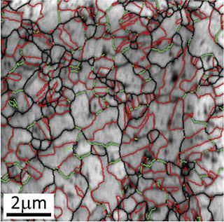
A nanostructured film is a film resulting from engineering of nanoscale features, such as dislocations, grain boundaries, defects, or twinning. In contrast to other nanostructures, such as nanoparticles, the film itself may be up to several microns thick, but possesses a large concentration of nanoscale features homogeneously distributed throughout the film. Like other nanomaterials, nanostructured films have sparked much interest as they possess unique properties not found in bulk, non-nanostructured material of the same composition. In particular, nanostructured films have been the subject of recent research due to their superior mechanical properties, including strength, hardness, and corrosion resistance compared to regular films of the same material. Examples of nanostructured films include those produced by grain boundary engineering, such as nano-twinned ultra-fine grain copper, or dual phase nanostructuring, such as crystalline metal and amorphous metallic glass nanocomposites.

The characterization of nanoparticles is a branch of nanometrology that deals with the characterization, or measurement, of the physical and chemical properties of nanoparticles. Nanoparticles measure less than 100 nanometers in at least one of their external dimensions, and are often engineered for their unique properties. Nanoparticles are unlike conventional chemicals in that their chemical composition and concentration are not sufficient metrics for a complete description, because they vary in other physical properties such as size, shape, surface properties, crystallinity, and dispersion state.

Purushottam Chakraborty is an Indian physicist who is one of the renowned experts in materials analysis using ion beams and secondary ion mass spectrometry (SIMS).

The "Centre d’Élaboration de Matériaux et d’Etudes Structurales" (CEMES) is a CNRS laboratory located in Toulouse, France.
| | This nanotechnology-related article is a stub. You can help Wikipedia by expanding it. |