JST connector

Last updated
2.50mm JST-XH top-entry (vertical) male PCB connectors Balancer Buchse XH.JPG
2.50mm JST-XH top-entry (vertical) male PCB connectors

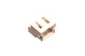
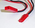
JST connectors are electrical connectors manufactured to the design standards originally developed by J.S.T. Mfg. Co. (Japan Solderless Terminal). [1] JST manufactures numerous series (families) and pitches (pin-to-pin distance) of connectors. [2] [3]

Contents

JST connectors are used in many types of products, and commonly used by electronics hobbyists and consumer products for rechargeable battery packs, battery balancers, battery eliminator circuits, 3D printers, and radio controlled servos. [4]

The term "JST" is sometimes incorrectly used as a vernacular term meaning any small white electrical connector mounted on PCBs.

Connector series

JST manufactures a large number of series (families) of connectors. [2] The PCB (wire-to-board) connectors are available in top (vertical) or side (horizontal) entry, and through-hole or surface-mount.

Wire-to-board connectors
JST seriesPin-to-pin pitchPin rows Current
(Amp)
Voltage
(Volt)
Wire size
(AWG)
ShroudLockNotesDatasheet
VH [5]
3.96  mm (0.156  in)
1
10
250
22 to 16
Yes/NoYesUnshrouded seems to be more popular than shrouded. JST VH
RE [6]
2.54 mm (0.100 in)
1
2
250
30 to 24
NoNoSimilar to female "DuPont" connectors and male pin headers. RF series is double row. [7] JST RE
EH [8]
2.50 mm (0.098 in)
1
3
250
32 to 22
YesNoNot 0.1-inch pitch. JST EH
XA [9]
2.50 mm (0.098 in)
1
3
250
30 to 20
YesYesNot 0.1-inch pitch. JST XA
XH [10]
2.50 mm (0.098 in)
1
3
250
30 to 22
YesYesNot 0.1-inch pitch. Used by many radio control (R/C) batteries. JST XH
PA [11]
2.00 mm (0.079 in)
1
3
250
28 to 22
YesYesUsed by FMA Cellpro R/C battery chargers. JST PA
PH [12]
2.00 mm (0.079 in)
1
2
100
32 to 24
YesNoMany stepper motors. Compatible with KR (IDC), KRD (IDC), CR (IDC) series. [13] [14] [15] JST PH
ZH [16]
1.50 mm (0.059 in)
1
1
50
32 to 26
YesNoCompatible with ZR (IDC) and ZM (crimp) series. [17] [18] JST ZH
GH [19]
1.25 mm (0.049 in)
1
1
50
30 to 26
YesYesNot 0.05-inch pitch. Sometimes confused with Molex PicoBlade. [20] JST GH
SH [21]
1.00 mm (0.039 in)
1
1
50
32 to 28
YesNoCompatible with SR (IDC) and SZ (IDC) series. [22] JST SH
Wire-to-wire connectors
JST seriesPin-to-pin pitchPin rows Current
(Amp)
Voltage
(Volt)
Wire size
(AWG)
FeaturesNotesDatasheet
RCY [23]
2.50  mm (0.098  in)
1
3
250
28 to 22
LockingUsed in radio control (R/C), also known as BEC or P connector. Commonly found on small models, toys, and small LiPo packs. JST RCY
SM [24]
2.50 mm (0.098 in)
1
3
250
28 to 22
Locking, High forceUsed in some RGB LED decorative light strips. JST SM

Connector soldering

A majority of JST through-hole headers can't withstand the temperatures required for reflow soldering, because the plastic has a lower melting point since they were designed for wave soldering methods. Some JST surface-mount headers are designed to handle higher temperatures of reflow soldering. [25]

Connector confusion on the internet

End-users and 3rd-party sellers on eBay often describe connectors by their wrong name thus perpetuating confusion of the exact series of a specific connector. It is very common in blogs and websites to incorrectly name a specific connector only by the name of the manufacturer.

To minimize confusion, it is best to describe a connector using: the manufacturer's name, exact connector series, and optionally the pitch, such as "JST-XH" or "JST-XH-2.50mm" or "2.50mm JST XH-series" or other variations.

The official J.S.T. Co. website has a tool which allows users to check certain models for their authenticity and specifications. [26]

Note: Some 2.50 mm parts are incorrectly sold on the internet as 2.54 mm (0.100 in), and the 1.25 mm parts as 1.27 mm (0.050 in).

See also

Related Research Articles

Dual in-line package Type of electronic component package

In microelectronics, a dual in-line package, is an electronic component package with a rectangular housing and two parallel rows of electrical connecting pins. The package may be through-hole mounted to a printed circuit board (PCB) or inserted in a socket. The dual-inline format was invented by Don Forbes, Rex Rice and Bryant Rogers at Fairchild R&D in 1964, when the restricted number of leads available on circular transistor-style packages became a limitation in the use of integrated circuits. Increasingly complex circuits required more signal and power supply leads ; eventually microprocessors and similar complex devices required more leads than could be put on a DIP package, leading to development of higher-density chip carriers. Furthermore, square and rectangular packages made it easier to route printed-circuit traces beneath the packages.

<span class="mw-page-title-main">Printed circuit board</span> Board to support and connect electronic components

A printed circuit board is a medium used in electrical and electronic engineering to connect electronic components to one another in a controlled manner. It takes the form of a laminated sandwich structure of conductive and insulating layers: each of the conductive layers is designed with an artwork pattern of traces, planes and other features etched from one or more sheet layers of copper laminated onto and/or between sheet layers of a non-conductive substrate. Electrical components may be fixed to conductive pads on the outer layers in the shape designed to accept the component's terminals, generally by means of soldering, to both electrically connect and mechanically fasten them to it. Another manufacturing process adds vias: plated-through holes that allow interconnections between layers.

Point-to-point construction Wiring of electronic circuitory without the use of a pcb

Point-to-point construction is a non-automated method of construction of electronics circuits widely used before the use of printed circuit boards (PCBs) and automated assembly gradually became widespread following their introduction in the 1950s. Circuits using thermionic valves were relatively large, relatively simple, and used large sockets, all of which made the PCB less obviously advantageous than with later complex semiconductor circuits. Point-to-point construction is still widespread in power electronics where components are bulky and serviceability is a consideration, and to construct prototype equipment with few or heavy electronic components. A common practice, especially in older point-to-point construction, is to use the leads of components such as resistors and capacitors to bridge as much of the distance between connections as possible, reducing the need to add additional wire between the components.

<span class="mw-page-title-main">Breadboard</span> Board with embedded spring clips that allows for electronics to be wired without soldering

A breadboard, solderless breadboard, protoboard, or terminal array board is a construction base used to build semi-permanent prototypes of electronic circuits. Unlike stripboard (Veroboard), breadboards do not require soldering or destruction to tracks and are hence reusable. For this reason, breadboards are also popular with students and in technological education.

Electrical connector Device used to join electrical conductors

Components of an electrical circuit are electrically connected if an electric current can run between them through an electrical conductor. An electrical connector is an electromechanical device used to create an electrical connection between parts of an electrical circuit, or between different electrical circuits, thereby joining them into a larger circuit. Most electrical connectors have a gender – i.e. the male component, called a plug, connects to the female component, or socket. The connection may be removable, require a tool for assembly and removal, or serve as a permanent electrical joint between two points. An adapter can be used to join dissimilar connectors.

Ribbon cable

A ribbon cable is a cable with many conducting wires running parallel to each other on the same flat plane. As a result, the cable is wide and flat. Its name comes from its resemblance to a piece of ribbon.

Ball grid array Surface-mount packaging that uses an array of solder balls

A ball grid array (BGA) is a type of surface-mount packaging used for integrated circuits. BGA packages are used to permanently mount devices such as microprocessors. A BGA can provide more interconnection pins than can be put on a dual in-line or flat package. The whole bottom surface of the device can be used, instead of just the perimeter. The traces connecting the package's leads to the wires or balls which connect the die to package are also on average shorter than with a perimeter-only type, leading to better performance at high speeds.

Surface-mount technology Method for producing electronic circuits

Surface-mount technology (SMT) is a method in which the electrical components are mounted directly onto the surface of a printed circuit board (PCB). An electrical component mounted in this manner is referred to as a surface-mount device (SMD). In industry, this approach has largely replaced the through-hole technology construction method of fitting components, in large part because SMT allows for increased manufacturing automation which reduces cost and improves quality. It also allows for more components to fit on a given area of substrate. Both technologies can be used on the same board, with the through-hole technology often used for components not suitable for surface mounting such as large transformers and heat-sinked power semiconductors.

Stripboard

Stripboard is the generic name for a widely used type of electronics prototyping material for circuit boards characterized by a pre-formed 0.1 inches (2.54 mm) regular (rectangular) grid of holes, with wide parallel strips of copper cladding running in one direction all the way across one side of on an insulating bonded paper board. It is commonly also known by the name of the original product Veroboard, which is a trademark, in the UK, of British company Vero Technologies Ltd and Canadian company Pixel Print Ltd. It was originated and developed in the early 1960s by the Electronics Department of Vero Precision Engineering Ltd (VPE). It was introduced as a general-purpose material for use in constructing electronic circuits - differing from purpose-designed printed circuit boards (PCBs) in that a variety of electronics circuits may be constructed using a standard wiring board.

<span class="mw-page-title-main">Flip chip</span> Technique that flips a microchip upside down to connect it

Flip chip, also known as controlled collapse chip connection or its abbreviation, C4, is a method for interconnecting dies such as semiconductor devices, IC chips, integrated passive devices and microelectromechanical systems (MEMS), to external circuitry with solder bumps that have been deposited onto the chip pads. The technique was developed by General Electric's Light Military Electronics Department, Utica, New York. The solder bumps are deposited on the chip pads on the top side of the wafer during the final wafer processing step. In order to mount the chip to external circuitry, it is flipped over so that its top side faces down, and aligned so that its pads align with matching pads on the external circuit, and then the solder is reflowed to complete the interconnect. This is in contrast to wire bonding, in which the chip is mounted upright and fine wires are welded onto the chip pads and lead frame contacts to interconnect the chip pads to external circuitry.

<span class="mw-page-title-main">D-subminiature</span> Type of electrical connector

The D-subminiature or D-sub is a common type of electrical connector. They are named for their characteristic D-shaped metal shield. When they were introduced, D-subs were among the smallest connectors used on computer systems.

<span class="mw-page-title-main">Wave soldering</span>

Wave soldering is a bulk soldering process used for the manufacturing of printed circuit boards. The circuit board is passed over a pan of molten solder in which a pump produces an upwelling of solder that looks like a standing wave. As the circuit board makes contact with this wave, the components become soldered to the board. Wave soldering is used for both through-hole printed circuit assemblies, and surface mount. In the latter case, the components are glued onto the surface of a printed circuit board (PCB) by placement equipment, before being run through the molten solder wave. Wave soldering is mainly used in soldering of through hole components.

Reflow soldering Attachment of electronic components

Reflow soldering is a process in which a solder paste is used to temporarily attach one or thousands of tiny electrical components to their contact pads, after which the entire assembly is subjected to controlled heat. The solder paste reflows in a molten state, creating permanent solder joints. Heating may be accomplished by passing the assembly through a reflow oven, under an infrared lamp, or (unconventionally) by soldering individual joints with a desoldering hot air pencil.

Berg connector Brand of electrical connector used in computer hardware

Berg connector is a brand of electrical connector used in computer hardware. Berg connectors are manufactured by Berg Electronics Corporation of St. Louis, Missouri, now part of Amphenol.

Selective soldering

Selective soldering is the process of selectively soldering components to printed circuit boards and molded modules that could be damaged by the heat of a reflow oven or wave soldering in a traditional surface-mount technology (SMT) or through-hole technology assembly processes. This usually follows an SMT oven reflow process; parts to be selectively soldered are usually surrounded by parts that have been previously soldered in a surface-mount reflow process, and the selective-solder process must be sufficiently precise to avoid damaging them.

Flat no-leads package Integrated circuit package with contacts on all 4 sides, on the underside of the package

Flat no-leads packages such as quad-flat no-leads (QFN) and dual-flat no-leads (DFN) physically and electrically connect integrated circuits to printed circuit boards. Flat no-leads, also known as micro leadframe (MLF) and SON, is a surface-mount technology, one of several package technologies that connect ICs to the surfaces of PCBs without through-holes. Flat no-lead is a near chip scale plastic encapsulated package made with a planar copper lead frame substrate. Perimeter lands on the package bottom provide electrical connections to the PCB. Flat no-lead packages include an exposed thermally conductive pad to improve heat transfer out of the IC. Heat transfer can be further facilitated by metal vias in the thermal pad. The QFN package is similar to the quad-flat package (QFP), and a ball grid array (BGA).

Automated optical inspection (AOI) is an automated visual inspection of printed circuit board (PCB) manufacture where a camera autonomously scans the device under test for both catastrophic failure and quality defects. It is commonly used in the manufacturing process because it is a non-contact test method. It is implemented at many stages through the manufacturing process including bare board inspection, solder paste inspection (SPI), pre-reflow and post-reflow as well as other stages.

Bead probe technology Technique used for in-circuit testing

Bead probe technology (BPT) is technique used to provide electrical access to printed circuit board (PCB) circuitry for performing in-circuit testing (ICT). It makes use of small beads of solder placed onto the board's traces to allow measuring and controlling of the signals using a test probe. This permits test access to boards on which standard ICT test pads are not feasible due to space constraints.

Pin header Type of simple electrical connector

A pin header is a form of electrical connector. A male pin header consists of one or more rows of metal pins molded into a plastic base, often 2.54 mm (0.1 in) apart, though available in many spacings. Male pin headers are cost-effective due to their simplicity. The female counterparts are sometimes known as female socket headers, though there are numerous naming variations of male and female connectors. Historically, headers have sometimes been called "Berg connectors", but headers are manufactured by many companies.

References

  1. "JST Corporate Profile and History". JST. Archived from the original on 27 November 2016. Retrieved 13 June 2017.
  2. 1 2 List of JST connector series; JST.
  3. Search by connector application; JST.
  4. "JST" connector confusion - the real story; rcgroups blog.
  5. JST VH-series webpage.
  6. JST RE-series webpage.
  7. JST RF-series webpage.
  8. JST EH-series webpage.
  9. JST XA-series webpage.
  10. JST XH-series webpage.
  11. JST PA-series webpage.
  12. JST PH-series webpage.
  13. JST KR-series webpage.
  14. JST KRD-series webpage.
  15. JST CR-series webpage.
  16. JST ZH-series webpage.
  17. JST ZR-series webpage.
  18. JST ZM-series webpage.
  19. JST GH-series webpage.
  20. JST Is Not A Connector
  21. JST SH-series webpage.
  22. JST SR/SZ-series webpage.
  23. JST RCY-series webpage.
  24. JST SM-series webpage.
  25. JST through-hole soldering; Official JST blog.
  26. "Choosing the Right JST Connector". DronesEtc. Archived from the original on 4 March 2016. Retrieved 13 August 2015.