A semiconductor device is an electronic component that exploits the electronic properties of semiconductor material, principally silicon, germanium, and gallium arsenide, as well as organic semiconductors. Semiconductor devices have replaced vacuum tubes in most applications. They use electrical conduction in the solid state rather that the gaseous state or thermionic emission in a vacuum.
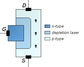
The junction gate field-effect transistor is one of the simple type of field-effect transistor. JFETs are three-terminal semiconductor devices that can be used as electronically-controlled switches, amplifiers, or voltage-controlled resistors.
N-type metal-oxide-semiconductor logic uses n-type field-effect transistors (MOSFETs) to implement logic gates and other digital circuits. These nMOS transistors operate by creating an inversion layer in a p-type transistor body. This inversion layer, called the n-channel, can conduct electrons between n-type "source" and "drain" terminals. The n-channel is created by applying voltage to the third terminal, called the gate. Like other MOSFETs, nMOS transistors have four modes of operation: cut-off, triode, saturation, and velocity saturation.
An insulated-gate bipolar transistor (IGBT) is a three-terminal power semiconductor device primarily used as an electronic switch which, as it was developed, came to combine high efficiency and fast switching. It consists of four alternating layers (P-N-P-N) that are controlled by a metal-oxide-semiconductor (MOS) gate structure without regenerative action. Although the structure of the IGBT is topologically the same as a thyristor with a 'MOS' gate, the thyristor action is completely suppressed and only the transistor action is permitted in the entire device operation range. It switches electric power in many applications: variable-frequency drives (VFDs), electric cars, trains, variable speed refrigerators, lamp ballasts, air-conditioners and even stereo systems with switching amplifiers.

A thyristor is a solid-state semiconductor device with four layers of alternating P- and N-type materials. It acts exclusively as a bistable switch, conducting when the gate receives a current trigger, and continuing to conduct until the voltage across the device is reversed biased, or until the voltage is removed. A three-lead thyristor is designed to control the larger current of the Anode to Cathode path by controlling that current with the smaller current of its other lead, known as its Gate. In contrast, a two-lead thyristor is designed to switch on if the potential difference between its leads is sufficiently large.

TRIAC, from triode for alternating current, is a generic trademark for a three terminal electronic component that conducts current in either direction when triggered. Its formal name is bidirectional triode thyristor or bilateral triode thyristor. A thyristor is analogous to a relay in that a small voltage induced current can control a much larger voltage and current. The illustration on the right shows the circuit symbol for a TRIAC where A1 is Anode 1, A2 is Anode 2, and G is Gate. Anode 1 and Anode 2 are normally termed Main Terminal 1 (MT1) and Main Terminal 2 (MT2) respectively.
A power semiconductor device is a semiconductor device used as a switch or rectifier in power electronics. Such a device is also called a power device or, when used in an integrated circuit, a power IC.

A High-electron-mobility transistor (HEMT), also known as heterostructure FET (HFET) or modulation-doped FET (MODFET), is a field-effect transistor incorporating a junction between two materials with different band gaps as the channel instead of a doped region. A commonly used material combination is GaAs with AlGaAs, though there is wide variation, dependent on the application of the device. Devices incorporating more indium generally show better high-frequency performance, while in recent years, gallium nitride HEMTs have attracted attention due to their high-power performance. Like other FETs, HEMTs are used in integrated circuits as digital on-off switches. FETs can also be used as amplifiers for large amounts of current using a small voltage as a control signal. Both of these uses are made possible by the FET’s unique current-voltage characteristics. HEMT transistors are able to operate at higher frequencies than ordinary transistors, up to millimeter wave frequencies, and are used in high-frequency products such as cell phones, satellite television receivers, voltage converters, and radar equipment. They are widely used in satellite receivers, in low power amplifiers and in the defense industry.

For power semiconductor devices, the safe operating area (SOA) is defined as the voltage and current conditions over which the device can be expected to operate without self-damage.
The static induction thyristor is a thyristor with a buried gate structure in which the gate electrodes are placed in n-base region. Since they are normally on-state, gate electrodes must be negatively or anode biased to hold off-state. It has low noise, low distortion, high audio frequency power capability. The turn-on and turn-off times are very short, typically 0.25 microseconds.

A power MOSFET is a specific type of metal oxide semiconductor field-effect transistor (MOSFET) designed to handle significant power levels.
Hot carrier injection (HCI) is a phenomenon in solid-state electronic devices where an electron or a “hole” gains sufficient kinetic energy to overcome a potential barrier necessary to break an interface state. The term "hot" refers to the effective temperature used to model carrier density, not to the overall temperature of the device. Since the charge carriers can become trapped in the gate dielectric of a MOS transistor, the switching characteristics of the transistor can be permanently changed. Hot-carrier injection is one of the mechanisms that adversely affects the reliability of semiconductors of solid-state devices.
An extrinsic semiconductor is one that has been doped; during manufacture of the semiconductor crystal a trace element or chemical called a doping agent has been incorporated chemically into the crystal, for the purpose of giving it different electrical properties than the pure semiconductor crystal, which is called an intrinsic semiconductor. In an extrinsic semiconductor it is these foreign dopant atoms in the crystal lattice that mainly provide the charge carriers which carry electric current through the crystal. The doping agents used are of two types, resulting in two types of extrinsic semiconductor. An electron donor dopant is an atom which, when incorporated in the crystal, releases a mobile conduction electron into the crystal lattice. An extrinsic semiconductor which has been doped with electron donor atoms is called an n-type semiconductor, because the majority of charge carriers in the crystal are negative electrons. An electron acceptor dopant is an atom which accepts an electron from the lattice, creating a vacancy where an electron should be called a hole which can move through the crystal like a positively charged particle. An extrinsic semiconductor which has been doped with electron acceptor atoms is called a p-type semiconductor, because the majority of charge carriers in the crystal are positive holes.
P-type metal-oxide-semiconductor logic uses p-channel metal-oxide-semiconductor field effect transistors (MOSFETs) to implement logic gates and other digital circuits. PMOS transistors operate by creating an inversion layer in an n-type transistor body. This inversion layer, called the p-channel, can conduct holes between p-type "source" and "drain" terminals.
Saturation velocity is the maximum velocity a charge carrier in a semiconductor, generally an electron, attains in the presence of very high electric fields.When this happens, the semiconductor is said to be in a state of velocity saturation. Charge carriers normally move at an average drift speed proportional to the electric field strength they experience temporally. The proportionality constant is known as mobility of the carrier, which is a material property. A good conductor would have a high mobility value for its charge carrier, which means higher velocity, and consequently higher current values for a given electric field strength. There is a limit though to this process and at some high field value, a charge carrier can not move any faster, having reached its saturation velocity, due to mechanisms that eventually limit the movement of the carriers in the material.
The following outline is provided as an overview of and topical guide to electronics:

The field-effect transistor (FET) is an electronic device which uses an electric field to control the flow of current. FETs are 3-terminalled devices, having a source, gate, and drain terminal. FETs control the flow of current by the application of a voltage to the gate terminal, which in turn alters the conductivity between the drain and source terminals.


