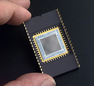
A charge-coupled device (CCD) is an integrated circuit containing an array of linked, or coupled, capacitors. Under the control of an external circuit, each capacitor can transfer its electric charge to a neighboring capacitor. CCD sensors are a major technology used in digital imaging.
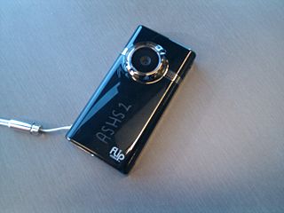
A video camera is an optical instrument that captures videos, as opposed to a movie camera, which records images on film. Video cameras were initially developed for the television industry but have since become widely used for a variety of other purposes.
A digital image is an image composed of picture elements, also known as pixels, each with finite, discrete quantities of numeric representation for its intensity or gray level that is an output from its two-dimensional functions fed as input by its spatial coordinates denoted with x, y on the x-axis and y-axis, respectively. Depending on whether the image resolution is fixed, it may be of vector or raster type. By itself, the term "digital image" usually refers to raster images or bitmapped images.

Photodetectors, also called photosensors, are sensors of light or other electromagnetic radiation. There are a wide variety of photodetectors which may be classified by mechanism of detection, such as photoelectric or photochemical effects, or by various performance metrics, such as spectral response. Semiconductor-based photodetectors typically use a p–n junction that converts photons into charge. The absorbed photons make electron–hole pairs in the depletion region. Photodiodes and photo transistors are a few examples of photo detectors. Solar cells convert some of the light energy absorbed into electrical energy.
Fluorescence-lifetime imaging microscopy or FLIM is an imaging technique based on the differences in the exponential decay rate of the photon emission of a fluorophore from a sample. It can be used as an imaging technique in confocal microscopy, two-photon excitation microscopy, and multiphoton tomography.
ams OSRAM AG is an Austrian semiconductor manufacturer headquartered in Premstätten, Austria with a co-headquarters in Munich, Germany. The company develops and produces intelligent sensors and emitter components

High-speed photography is the science of taking pictures of very fast phenomena. In 1948, the Society of Motion Picture and Television Engineers (SMPTE) defined high-speed photography as any set of photographs captured by a camera capable of 69 frames per second or greater, and of at least three consecutive frames. High-speed photography can be considered to be the opposite of time-lapse photography.

An image sensor or imager is a sensor that detects and conveys information used to form an image. It does so by converting the variable attenuation of light waves into signals, small bursts of current that convey the information. The waves can be light or other electromagnetic radiation. Image sensors are used in electronic imaging devices of both analog and digital types, which include digital cameras, camera modules, camera phones, optical mouse devices, medical imaging equipment, night vision equipment such as thermal imaging devices, radar, sonar, and others. As technology changes, electronic and digital imaging tends to replace chemical and analog imaging.

An active-pixel sensor (APS) is an image sensor, which was invented by Peter J.W. Noble in 1968, where each pixel sensor unit cell has a photodetector and one or more active transistors. In a metal–oxide–semiconductor (MOS) active-pixel sensor, MOS field-effect transistors (MOSFETs) are used as amplifiers. There are different types of APS, including the early NMOS APS and the now much more common complementary MOS (CMOS) APS, also known as the CMOS sensor. CMOS sensors are used in digital camera technologies such as cell phone cameras, web cameras, most modern digital pocket cameras, most digital single-lens reflex cameras (DSLRs), mirrorless interchangeable-lens cameras (MILCs), and lensless imaging for cells.
Chemical imaging is the analytical capability to create a visual image of components distribution from simultaneous measurement of spectra and spatial, time information. Hyperspectral imaging measures contiguous spectral bands, as opposed to multispectral imaging which measures spaced spectral bands.
OmniVision Technologies Inc. is an American subsidiary of Chinese semiconductor device and mixed-signal integrated circuit design house Will Semiconductor. The company designs and develops digital imaging products for use in mobile phones, laptops, netbooks webcams, security, entertainment, automotive and medical imaging systems. Headquartered in Santa Clara, California, OmniVision Technologies has offices in the US, Western Europe and Asia.

Oxford Instruments Andor Ltd is a global developer and manufacturer of scientific cameras, microscopy systems and spectrographs for academic, government, and industrial applications. Founded in 1989, the company's products play a central role in the advancement of research in the fields of life sciences, physical sciences, and industrial applications. Andor was purchased for £176 million in December 2013 by Oxford Instruments. The company is based in Belfast, Northern Ireland and now employs over 400 staff across the group at its offices in Belfast, Japan, China, Switzerland and the US.

A time-of-flight camera, also known as time-of-flight sensor, is a range imaging camera system for measuring distances between the camera and the subject for each point of the image based on time-of-flight, the round trip time of an artificial light signal, as provided by a laser or an LED. Laser-based time-of-flight cameras are part of a broader class of scannerless LIDAR, in which the entire scene is captured with each laser pulse, as opposed to point-by-point with a laser beam such as in scanning LIDAR systems. Time-of-flight camera products for civil applications began to emerge around 2000, as the semiconductor processes allowed the production of components fast enough for such devices. The systems cover ranges of a few centimeters up to several kilometers.

A back-illuminated sensor, also known as backside illumination (BI) sensor, is a type of digital image sensor that uses a novel arrangement of the imaging elements to increase the amount of light captured and thereby improve low-light performance.

PMD Technologies is a developer of CMOS semiconductor 3D time-of-flight (ToF) components and a provider of engineering support in the field of digital 3D imaging. The company is named after the Photonic Mixer Device (PMD) technology used in its products to detect 3D data in real time. The corporate headquarters of the company is located in Siegen, Germany.
sCMOS are a type of CMOS image sensor (CIS). These sensors are commonly used as components in specific observational scientific instruments, such as microscopes and telescopes. sCMOS image sensors offer extremely low noise, rapid frame rates, wide dynamic range, high quantum efficiency, high resolution, and a large field of view simultaneously in one image.

Vitesco Technologies Group AG, headquartered in Regensburg, is a German automotive supplier for drivetrain and powertrain technologies. Vitesco Technologies was a business area of Continental AG until it became independent in September 2021. The company develops devices for electric vehicles as well as internal combustion engines.

There are a variety of technologies available for detecting and recording the images, diffraction patterns, and electron energy loss spectra produced using transmission electron microscopy (TEM).
Gamaya is a Swiss company which provides drones equipped with hyper-spectral cameras for use in agriculture.

Single-pixel imaging is a computational imaging technique for producing spatially-resolved images using a single detector instead of an array of detectors. A device that implements such an imaging scheme is called a single-pixel camera. Combined with compressed sensing, the single-pixel camera can recover images from fewer measurements than the number of reconstructed pixels.