Semiconductor optical gain

Last updated

Optical gain is the most important requirement for the realization of a semiconductor laser because it describes the optical amplification in the semiconductor material. This optical gain is due to stimulated emission associated with light emission created by recombination of electrons and holes. While in other laser materials like in gas lasers or solid state lasers, the processes associated with optical gain are rather simple, in semiconductors this is a complex many-body problem of interacting photons, electrons, and holes. Accordingly, understanding these processes is a major objective as being a basic requirement for device optimization. This task can be solved by development of appropriate theoretical models to describe the semiconductor optical gain and by comparison of the predictions of these models with experimental results found.

Contents

Theory for optical gain in semiconductors

Since defining semiconductor's optical gain is an ambitious undertaking, it is useful to build the understanding by steps. The basic requirements can be defined without the major complications induced by the Coulomb interaction among electrons and holes. To explain the actual operation of semiconductor lasers, one must refine this analysis by systematically including the Coulomb-interaction effects.

Free-carrier picture

For a simple, qualitative understanding of optical gain and its spectral dependency, often so-called free-carrier models are used which is discussed considering the example of a bulk laser here. The term free carrier means that any interactions between the carriers are neglected. A free-carrier model provides the following expression for the spectral dependence [1] [2]

with the reduced-mass energy , the quasi-Fermi-distribution functions for the conduction-band and for the valence-band , respectively, and with given by: [1] [2]

with being the frequency, the dipole-matrix element, the reduced mass, the vacuum permittivity, and the refractive index.

Thus, the shape of the gain spectrum is determined by the density of states, proportional to , for bulk material and the quasi-Fermi-distribution functions. This expression gives a qualitative impression of the dependence of the gain spectra on the distribution functions. However, a comparison to experimental data shows immediately that this approach is not at all suited to give quantitative predictions on the exact gain values and the correct shape of the spectra. For that purpose, a microscopic model including many-body interactions is required. In recent years, the microscopic many-body model based on the semiconductor Bloch equations (SBE) has been very successful. [3] [4] [5] [6]

Microscopic many body gain model

The model is based on the SBE describing the dynamics of the microscopic polarizations between conduction and valence bands, the distribution functions , [1] and the many-body correlations created by the interactions.

If only stationary gain spectra in the linear regime are of interest, one can neglect the time dependence of the distribution functions and , and simply express them by quasi-Fermi-distributions for a given carrier density and temperature. The microscopic polarizations are given by:

where is the renormalized transition energy between conduction and valence bands and is the renormalized Rabi frequency.

In contrast to the free-carrier description, this model contains contributions due to many-body Coulomb interactions such as and , and the collision term that describes the effect of the correlations which may be treated in different approximations. The easiest approach is to replace the collision term by a phenomenological relaxation rate (-approximation). [1] However, though this approximation is often used, it leads to somewhat unphysical results like absorption below the semiconductor band gap. A more correct but also much more complex approach considers the collision term kinetically and thus contains in- and out-scattering rates for the microscopic polarizations. [2] In this quantum kinetic approach, the calculations require only the basic input parameters (material band structure, geometrical structure, and temperature) and provide the semiconductor gain and refractive index spectra without further free parameters.

In detail, the above-mentioned equation of motion of the polarization is solved numerically by calculating the first two terms on the right hand side from the input parameters and by computing the collision contributions. Then, the equation of motion is numerically time-integrated and the microscopic polarizations are summed over to obtain the complex macroscopic polarization which then provides the gain and the refractive index spectra in semiconductor laser theory. It should be mentioned that present-day modeling assumes a perfect semiconductor structure in order to reduce the numerical effort. Disorder effects like composition variations or thickness fluctuations of the material are not microscopically considered but such imperfections often occur in real structures. Such contributions to inhomogeneous broadening may be included into the theory by convolution with a Gaussian broadening function for quantitative comparison with experimental data.

Experimental determination of the optical gain

The predictive quality of microscopic modeling can be verified or disproved by optical-gain measurements. If the design is approved, one may continue to laser production. If experiments exhibit unexpected gain features, one can refine the modeling by including systematically new effects. As more effects are included, the predictive power of the model increases. In general, a closed-loop design, where the modeling and experiment are replaced cyclically, has proven to be a very efficient method to find and develop new laser designs with desired performance.

Stripe-length method

Various experimental approaches can be used for the determination of the optical gain of semiconductor structures. For example, the optical stripe-length method is widely applied. [7] This method uses a strong laser source for optical excitation of the sample under investigation. The laser beam is focused to a stripe (e.g., with a cylindrical lens) onto the sample such that the stripe covers the sample but extends to one of its edges. Then, the intensity of the amplified spontaneous emission (ASE) of the sample out of this edge is measured as a function of the stripe length . The gain can then be extracted from an appropriate fit of the data. The stripe-length method provides reasonable qualitative results for semiconductor samples which have not yet been processed towards electrically pumped laser structures. More quantitatively accurate results, however, are obtained with other methods that require completely processed laser structures that emit in the fundamental lateral mode only as, for example, the Hakki–Paoli method and the transmission method.

Hakki–Paoli method

For the Hakki–Paoli method, [8] the semiconductor laser has to be operated below the laser threshold. Then, the spectrum of the emitted ASE is strongly governed by the Fabry–Pérot modes of the diode laser resonator. If the length of the device and the reflectivities of the facets are known, the gain can be evaluated from the maxima and the minima of the Fabry–Pérot peaks in the ASE spectrum. This requires, however, that the ASE data are recorded with a spectrometer of sufficient spectral resolution. Then, this method is rather easy and straightforward but it provides gain data only in the regime below the laser threshold while in many cases the gain above the laser threshold would also be of interest, in particular for a quantitative comparison to a theoretical model.

Transmission method

The transmission method [3] requires a weak broadband light source that spectrally covers the region of interest for the gain spectra. This light source is transmitted through the device of interest and the ratio of the intensities after and before the laser device provides the gain spectra. [3] For this method, the device should operate on the fundamental lateral mode and the occurrence of Fabry–Pérot modes should be suppressed by deposition of at least one antireflection coating on the output facet of the device. In comparison to the stripe-length method and the Hakki–Paoli method, the transmission method provides the most accurate gain data for the widest range of injection currents. The Hakki–Paoli method can be directly compared to calculations within the Semiconductor Bloch equations.

Comparison of theory and experiment

The figure shows a comparison between experimental gain spectra for a (GaIn)(NAs)/GaAs quantum well ridge waveguide laser structure determined with the transmission method with gain spectra calculated with the microscopic many-body model. Gain spectrum of a GaIn NAs GaAs quantum well.png
The figure shows a comparison between experimental gain spectra for a (GaIn)(NAs)/GaAs quantum well ridge waveguide laser structure determined with the transmission method with gain spectra calculated with the microscopic many-body model.

The figure shows sets of theoretical and experimental gain spectra for a (GaIn)(NAs)/GaAs quantum-well structure. [4] For the experimental spectra, the injection current was varied while for the theoretical curves different carrier densities were considered. The theoretical spectra were convoluted with a Gaussian function with an inhomogeneous broadening of 19.7 meV. While for the data shown in the figure, the inhomogeneous broadening was adapted for optimum agreement with experiment, it may also unambiguously determined from low-density luminescence spectra of the material under study. [5] Almost perfect quantitative agreement of theoretical and experimental gain spectra can be obtained considering that the device heats up slightly in the experiment at higher injection currents. Thus, the temperature is increased for the gain spectra at higher carrier densities. Note that apart from that, there were no free fitting parameters entering the theory. Accordingly, once the material parameters are known, the microscopic many-body model provides an accurate prediction of the optical gain spectra of any new semiconductor material as, for example, (GaIn)(NAs)/GaAs [4] or Ga(NAsP)/Si. [6]

See also

Further reading

Related Research Articles

<span class="mw-page-title-main">Maxwell's equations</span> Equations describing classical electromagnetism

Maxwell's equations, or Maxwell–Heaviside equations, are a set of coupled partial differential equations that, together with the Lorentz force law, form the foundation of classical electromagnetism, classical optics, and electric circuits. The equations provide a mathematical model for electric, optical, and radio technologies, such as power generation, electric motors, wireless communication, lenses, radar etc. They describe how electric and magnetic fields are generated by charges, currents, and changes of the fields. The equations are named after the physicist and mathematician James Clerk Maxwell, who, in 1861 and 1862, published an early form of the equations that included the Lorentz force law. Maxwell first used the equations to propose that light is an electromagnetic phenomenon. The modern form of the equations in their most common formulation is credited to Oliver Heaviside.

<span class="mw-page-title-main">Nonlinear optics</span> Branch of physics

Nonlinear optics (NLO) is the branch of optics that describes the behaviour of light in nonlinear media, that is, media in which the polarization density P responds non-linearly to the electric field E of the light. The non-linearity is typically observed only at very high light intensities (when the electric field of the light is >108 V/m and thus comparable to the atomic electric field of ~1011 V/m) such as those provided by lasers. Above the Schwinger limit, the vacuum itself is expected to become nonlinear. In nonlinear optics, the superposition principle no longer holds.

<span class="mw-page-title-main">Refractive index</span> Ratio of the speed of light in vacuum to that in the medium

In optics, the refractive index of an optical medium is a dimensionless number that gives the indication of the light bending ability of that medium.

<span class="mw-page-title-main">Permittivity</span> Measure of the electric polarizability of a dielectric

In electromagnetism, the absolute permittivity, often simply called permittivity and denoted by the Greek letter ε (epsilon), is a measure of the electric polarizability of a dielectric. A material with high permittivity polarizes more in response to an applied electric field than a material with low permittivity, thereby storing more energy in the material. In electrostatics, the permittivity plays an important role in determining the capacitance of a capacitor.

<span class="mw-page-title-main">Photoluminescence</span> Light emission from substances after they absorb photons

Photoluminescence is light emission from any form of matter after the absorption of photons. It is one of many forms of luminescence and is initiated by photoexcitation, hence the prefix photo-. Following excitation, various relaxation processes typically occur in which other photons are re-radiated. Time periods between absorption and emission may vary: ranging from short femtosecond-regime for emission involving free-carrier plasma in inorganic semiconductors up to milliseconds for phosphoresence processes in molecular systems; and under special circumstances delay of emission may even span to minutes or hours.

In physics, screening is the damping of electric fields caused by the presence of mobile charge carriers. It is an important part of the behavior of charge-carrying fluids, such as ionized gases, electrolytes, and charge carriers in electronic conductors . In a fluid, with a given permittivity ε, composed of electrically charged constituent particles, each pair of particles interact through the Coulomb force as

<span class="mw-page-title-main">Ampère's circuital law</span> Concept in classical electromagnetism

In classical electromagnetism, Ampère's circuital law relates the integrated magnetic field around a closed loop to the electric current passing through the loop. James Clerk Maxwell derived it using hydrodynamics in his 1861 published paper "On Physical Lines of Force" In 1865 he generalized the equation to apply to time-varying currents by adding the displacement current term, resulting in the modern form of the law, sometimes called the Ampère–Maxwell law, which is one of Maxwell's equations which form the basis of classical electromagnetism.

Space charge is an interpretation of a collection of electric charges in which excess electric charge is treated as a continuum of charge distributed over a region of space rather than distinct point-like charges. This model typically applies when charge carriers have been emitted from some region of a solid—the cloud of emitted carriers can form a space charge region if they are sufficiently spread out, or the charged atoms or molecules left behind in the solid can form a space charge region.

The Kerr effect, also called the quadratic electro-optic (QEO) effect, is a change in the refractive index of a material in response to an applied electric field. The Kerr effect is distinct from the Pockels effect in that the induced index change is directly proportional to the square of the electric field instead of varying linearly with it. All materials show a Kerr effect, but certain liquids display it more strongly than others. The Kerr effect was discovered in 1875 by Scottish physicist John Kerr.

<span class="mw-page-title-main">Polarization density</span> Vector field describing the density of electric dipole moments in a dielectric material

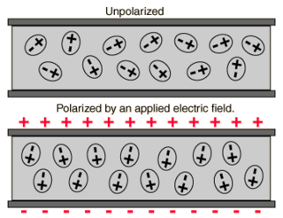
In classical electromagnetism, polarization density is the vector field that expresses the density of permanent or induced electric dipole moments in a dielectric material. When a dielectric is placed in an external electric field, its molecules gain electric dipole moment and the dielectric is said to be polarized. The electric dipole moment induced per unit volume of the dielectric material is called the electric polarization of the dielectric.

In plasmas and electrolytes, the Debye length, is a measure of a charge carrier's net electrostatic effect in a solution and how far its electrostatic effect persists. With each Debye length the charges are increasingly electrically screened and the electric potential decreases in magnitude by 1/e. A Debye sphere is a volume whose radius is the Debye length. Debye length is an important parameter in plasma physics, electrolytes, and colloids. The corresponding Debye screening wave vector for particles of density , charge at a temperature is given by in Gaussian units. Expressions in MKS units will be given below. The analogous quantities at very low temperatures are known as the Thomas–Fermi length and the Thomas–Fermi wave vector. They are of interest in describing the behaviour of electrons in metals at room temperature.

Free carrier absorption occurs when a material absorbs a photon, and a carrier is excited from an already-excited state to another, unoccupied state in the same band. This intraband absorption is different from interband absorption because the excited carrier is already in an excited band, such as an electron in the conduction band or a hole in the valence band, where it is free to move. In interband absorption, the carrier starts in a fixed, nonconducting band and is excited to a conducting one.

Heat transfer physics describes the kinetics of energy storage, transport, and energy transformation by principal energy carriers: phonons, electrons, fluid particles, and photons. Heat is energy stored in temperature-dependent motion of particles including electrons, atomic nuclei, individual atoms, and molecules. Heat is transferred to and from matter by the principal energy carriers. The state of energy stored within matter, or transported by the carriers, is described by a combination of classical and quantum statistical mechanics. The energy is different made (converted) among various carriers. The heat transfer processes are governed by the rates at which various related physical phenomena occur, such as the rate of particle collisions in classical mechanics. These various states and kinetics determine the heat transfer, i.e., the net rate of energy storage or transport. Governing these process from the atomic level to macroscale are the laws of thermodynamics, including conservation of energy.

The semiconductor Bloch equations describe the optical response of semiconductors excited by coherent classical light sources, such as lasers. They are based on a full quantum theory, and form a closed set of integro-differential equations for the quantum dynamics of microscopic polarization and charge carrier distribution. The SBEs are named after the structural analogy to the optical Bloch equations that describe the excitation dynamics in a two-level atom interacting with a classical electromagnetic field. As the major complication beyond the atomic approach, the SBEs must address the many-body interactions resulting from Coulomb force among charges and the coupling among lattice vibrations and electrons.

The semiconductor luminescence equations (SLEs) describe luminescence of semiconductors resulting from spontaneous recombination of electronic excitations, producing a flux of spontaneously emitted light. This description established the first step toward semiconductor quantum optics because the SLEs simultaneously includes the quantized light–matter interaction and the Coulomb-interaction coupling among electronic excitations within a semiconductor. The SLEs are one of the most accurate methods to describe light emission in semiconductors and they are suited for a systematic modeling of semiconductor emission ranging from excitonic luminescence to lasers.

The Elliott formula describes analytically, or with few adjustable parameters such as the dephasing constant, the light absorption or emission spectra of solids. It was originally derived by Roger James Elliott to describe linear absorption based on properties of a single electron–hole pair. The analysis can be extended to a many-body investigation with full predictive powers when all parameters are computed microscopically using, e.g., the semiconductor Bloch equations or the semiconductor luminescence equations.

The interaction of matter with light, i.e., electromagnetic fields, is able to generate a coherent superposition of excited quantum states in the material. Coherent denotes the fact that the material excitations have a well defined phase relation which originates from the phase of the incident electromagnetic wave. Macroscopically, the superposition state of the material results in an optical polarization, i.e., a rapidly oscillating dipole density. The optical polarization is a genuine non-equilibrium quantity that decays to zero when the excited system relaxes to its equilibrium state after the electromagnetic pulse is switched off. Due to this decay which is called dephasing, coherent effects are observable only for a certain temporal duration after pulsed photoexcitation. Various materials such as atoms, molecules, metals, insulators, semiconductors are studied using coherent optical spectroscopy and such experiments and their theoretical analysis has revealed a wealth of insights on the involved matter states and their dynamical evolution.

<span class="mw-page-title-main">Semiconductor laser theory</span> Theory of laser diodes

Semiconductor lasers or laser diodes play an important part in our everyday lives by providing cheap and compact-size lasers. They consist of complex multi-layer structures requiring nanometer scale accuracy and an elaborate design. Their theoretical description is important not only from a fundamental point of view, but also in order to generate new and improved designs. It is common to all systems that the laser is an inverted carrier density system. The carrier inversion results in an electromagnetic polarization which drives an electric field . In most cases, the electric field is confined in a resonator, the properties of which are also important factors for laser performance.

The Wannier equation describes a quantum mechanical eigenvalue problem in solids where an electron in a conduction band and an electronic vacancy within a valence band attract each other via the Coulomb interaction. For one electron and one hole, this problem is analogous to the Schrödinger equation of the hydrogen atom; and the bound-state solutions are called excitons. When an exciton's radius extends over several unit cells, it is referred to as a Wannier exciton in contrast to Frenkel excitons whose size is comparable with the unit cell. An excited solid typically contains many electrons and holes; this modifies the Wannier equation considerably. The resulting generalized Wannier equation can be determined from the homogeneous part of the semiconductor Bloch equations or the semiconductor luminescence equations.

<span class="mw-page-title-main">Lorentz oscillator model</span> Theoretical model describing the optical response of bound charges

The Lorentz oscillator model describes the optical response of bound charges. The model is named after the Dutch physicist Hendrik Antoon Lorentz. It is a classical, phenomenological model for materials with characteristic resonance frequencies for optical absorption, e.g. ionic and molecular vibrations, interband transitions (semiconductors), phonons, and collective excitations.

References

  1. 1 2 3 4 Chow, W. W.; Koch, S. W.; Sargent, M. (1994). Semiconductor-laser physics. Springer-Verlag. ISBN   978-3-540-57614-3.
  2. 1 2 3 Chow, W. W.; Koch, S. W. (27 August 1999). Semiconductor-Laser Fundamentals: Physics of the Gain Materials. Springer. ISBN   978-3-540-64166-7.
  3. 1 2 3 Ellmers, C.; Girndt, A.; Hofmann, M.; Knorr, A.; Rühle, W. W.; Jahnke, F.; Koch, S. W.; Hanke, C.; Korte, L.; Hoyler, C. (1998). "Measurement and calculation of gain spectra for (GaIn)As/(AlGa)As single quantum well lasers". Applied Physics Letters72 (13): 1647. doi : 10.1063/1.121140. ISSN   0003-6951.
  4. 1 2 3 Hofmann, M.R.; Gerhardt, N.; Wagner, A. M.; Ellmers, C.; Hohnsdorf, F.; Koch, J.; Stolz, W.; Koch, S. W.; Ruhle, W. W.; Hader, J.; Moloney, J. V.; O'Reilly, E.P.; Borchert, B.; Egorov, A.Y.; Riechert, H.; Schneider, H. C.; Chow, W. W. (2002). "Emission dynamics and optical gain of 1.3-μm (GaIn)(NAs)/GaAs lasers". IEEE Journal of Quantum Electronics38 (2): 213–221. doi : 10.1109/3.980275. ISSN   0018-9197.
  5. 1 2 Hader, J.; Zakharian, A. R.; Moloney, J. V.; Nelson, T. R.; Siskaninetz, W. J.; Ehret, J. E.; Hantke, K.; Hofmann, M. et al. (2002). "Quantitative prediction of semiconductor laser characteristics based on low intensity photoluminescence measurements". IEEE Photonics Technology Letters14 (6): 762–764. doi : 10.1109/LPT.2002.1003085. ISSN   1041-1135.
  6. 1 2 Koukourakis, N.; Bückers, C.; Funke, D. A.; Gerhardt, N. C.; Liebich, S.; Chatterjee, S.; Lange, C.; Zimprich, M.; Volz, K.; Stolz, W.; Kunert, B.; Koch, S. W.; Hofmann, M. R. (2012). "High room-temperature optical gain in Ga(NAsP)/Si heterostructures". Applied Physics Letters100 (9): 092107. doi : 10.1063/1.3690886. ISSN   0003-6951.
  7. Hvam, J. M. (1978). "Direct recording of optical-gain spectra from ZnO". Journal of Applied Physics49 (6): 3124. doi : 10.1063/1.325304. ISSN   0021-8979.
  8. Hakki, B. W. (1973). "cw degradation at 300K of GaAs double-heterostructure junction lasers. II. Electronic gain". Journal of Applied Physics44 (9): 4113. doi : 10.1063/1.1662905. ISSN   0021-8979.