
Chemical vapor deposition (CVD) is a vacuum deposition method used to produce high-quality, and high-performance, solid materials. The process is often used in the semiconductor industry to produce thin films.

Gallium arsenide (GaAs) is a III-V direct band gap semiconductor with a zinc blende crystal structure.

Silicon carbide (SiC), also known as carborundum, is a hard chemical compound containing silicon and carbon. A semiconductor, it occurs in nature as the extremely rare mineral moissanite, but has been mass-produced as a powder and crystal since 1893 for use as an abrasive. Grains of silicon carbide can be bonded together by sintering to form very hard ceramics that are widely used in applications requiring high endurance, such as car brakes, car clutches and ceramic plates in bulletproof vests. Large single crystals of silicon carbide can be grown by the Lely method and they can be cut into gems known as synthetic moissanite.

Epitaxy refers to a type of crystal growth or material deposition in which new crystalline layers are formed with one or more well-defined orientations with respect to the crystalline seed layer. The deposited crystalline film is called an epitaxial film or epitaxial layer. The relative orientation(s) of the epitaxial layer to the seed layer is defined in terms of the orientation of the crystal lattice of each material. For most epitaxial growths, the new layer is usually crystalline and each crystallographic domain of the overlayer must have a well-defined orientation relative to the substrate crystal structure. Epitaxy can involve single-crystal structures, although grain-to-grain epitaxy has been observed in granular films. For most technological applications, single-domain epitaxy, which is the growth of an overlayer crystal with one well-defined orientation with respect to the substrate crystal, is preferred. Epitaxy can also play an important role while growing superlattice structures.
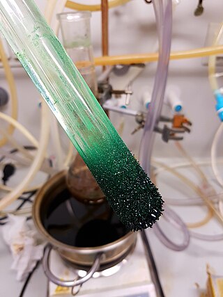
Sublimation is the transition of a substance directly from the solid to the gas state, without passing through the liquid state. The verb form of sublimation is sublime, or less preferably, sublimate. Sublimate also refers to the product obtained by sublimation. The point at which sublimation occurs rapidly is called critical sublimation point, or simply sublimation point. Notable examples include sublimation of dry ice at room temperature and atmospheric pressure, and that of solid iodine with heating.
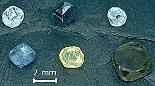
Laboratory-grown (LGD), also called lab-grown diamond, laboratory-created, man-made, artisan-created, artificial, synthetic, or cultured diamond, is diamond that is produced in a controlled technological process. Unlike diamond simulants, synthetic diamonds are composed of the same material as naturally formed diamonds—pure carbon crystallized in an isotropic 3D form—and share identical chemical and physical properties. As of 2023 the heaviest synthetic diamond ever made weighs 30.18 ct, and the heaviest natural diamond ever found weighs 3167 ct.

Tungsten(VI) fluoride, also known as tungsten hexafluoride, is an inorganic compound with the formula WF6. It is a toxic, corrosive, colorless gas, with a density of about 13 kg/m3 (22 lb/cu yd). It is the only known gaseous transition metal compound and the densest known gas under standard ambient temperature and pressure. WF6 is commonly used by the semiconductor industry to form tungsten films, through the process of chemical vapor deposition. This layer is used in a low-resistivity metallic "interconnect". It is one of seventeen known binary hexafluorides.
A boule is a single-crystal ingot produced by synthetic means.

A superalloy, or high-performance alloy, is an alloy with the ability to operate at a high fraction of its melting point. Key characteristics of a superalloy include mechanical strength, thermal creep deformation resistance, surface stability, and corrosion and oxidation resistance.
In materials science, a single crystal is a material in which the crystal lattice of the entire sample is continuous and unbroken to the edges of the sample, with no grain boundaries. The absence of the defects associated with grain boundaries can give monocrystals unique properties, particularly mechanical, optical and electrical, which can also be anisotropic, depending on the type of crystallographic structure. These properties, in addition to making some gems precious, are industrially used in technological applications, especially in optics and electronics.
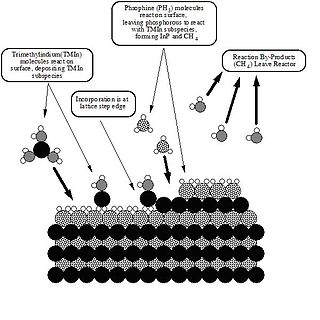
Metalorganic vapour-phase epitaxy (MOVPE), also known as organometallic vapour-phase epitaxy (OMVPE) or metalorganic chemical vapour deposition (MOCVD), is a chemical vapour deposition method used to produce single- or polycrystalline thin films. It is a process for growing crystalline layers to create complex semiconductor multilayer structures. In contrast to molecular-beam epitaxy (MBE), the growth of crystals is by chemical reaction and not physical deposition. This takes place not in vacuum, but from the gas phase at moderate pressures. As such, this technique is preferred for the formation of devices incorporating thermodynamically metastable alloys, and it has become a major process in the manufacture of optoelectronics, such as Light-emitting diodes, its most widespread application. It was first demonstrated in 1967 at North American Aviation Autonetics Division in Anaheim CA by Harold M. Manasevit.
Electron-beam physical vapor deposition, or EBPVD, is a form of physical vapor deposition in which a target anode is bombarded with an electron beam given off by a charged tungsten filament under high vacuum. The electron beam causes atoms from the target to transform into the gaseous phase. These atoms then precipitate into solid form, coating everything in the vacuum chamber with a thin layer of the anode material.
Physical vapor deposition (PVD), sometimes called physical vapor transport (PVT), describes a variety of vacuum deposition methods which can be used to produce thin films and coatings on substrates including metals, ceramics, glass, and polymers. PVD is characterized by a process in which the material transitions from a condensed phase to a vapor phase and then back to a thin film condensed phase. The most common PVD processes are sputtering and evaporation. PVD is used in the manufacturing of items which require thin films for optical, mechanical, electrical, acoustic or chemical functions. Examples include semiconductor devices such as thin-film solar cells, microelectromechanical devices such as thin film bulk acoustic resonator, aluminized PET film for food packaging and balloons, and titanium nitride coated cutting tools for metalworking. Besides PVD tools for fabrication, special smaller tools used mainly for scientific purposes have been developed.
A micropipe, also called a micropore, microtube, capillary defect or pinhole defect, is a crystallographic defect in a single crystal substrate. Minimizing the presence of micropipes is important in semiconductor manufacturing, as their presence on a wafer can result in the failure of integrated circuits made from that wafer.
Monocrystalline silicon, more often called single-crystal silicon, in short mono c-Si or mono-Si, is the base material for silicon-based discrete components and integrated circuits used in virtually all modern electronic equipment. Mono-Si also serves as a photovoltaic, light-absorbing material in the manufacture of solar cells.

The vapor–liquid–solid method (VLS) is a mechanism for the growth of one-dimensional structures, such as nanowires, from chemical vapor deposition. The growth of a crystal through direct adsorption of a gas phase on to a solid surface is generally very slow. The VLS mechanism circumvents this by introducing a catalytic liquid alloy phase which can rapidly adsorb a vapor to supersaturation levels, and from which crystal growth can subsequently occur from nucleated seeds at the liquid–solid interface. The physical characteristics of nanowires grown in this manner depend, in a controllable way, upon the size and physical properties of the liquid alloy.
Ultra-high-purity steam, also called the clean steam, UHP steam or high purity water vapor, is used in a variety of industrial manufacturing processes that require oxidation or annealing. These processes include the growth of oxide layers on silicon wafers for the semiconductor industry, originally described by the Deal-Grove model, and for the formation of passivation layers used to improve the light capture ability of crystalline photovoltaic cells. Several methods and technologies can be employed to generate ultra high purity steam, including pyrolysis, bubbling, direct liquid injection, and purified steam generation. The level of purity, or the relative lack of contamination, affects the quality of the oxide layer or annealed surface. The method of delivery affects growth rate, uniformity, and electrical performance. Oxidation and annealing are common steps in the manufacture of such devices as microelectronics and solar cells.

The Lely method, also known as the Lely process or Lely technique, is a crystal growth technology used for producing silicon carbide crystals for the semiconductor industry. The patent for this method was filed in the Netherlands in 1954 and in the United States in 1955 by Jan Anthony Lely of Philips Electronics. The patent was subsequently granted on 30 September 1958, then was refined by D. R. Hamilton et al. in 1960, and by V. P. Novikov and V. I. Ionov in 1968.
A rapidly increasing list of graphene production techniques have been developed to enable graphene's use in commercial applications.
Epitaxial graphene growth on silicon carbide (SiC) by thermal decomposition is a method to produce large-scale few-layer graphene (FLG). Graphene is one of the most promising nanomaterials for the future because of its various characteristics, like strong stiffness and high electric and thermal conductivity. Still, reproducible production of Graphene is difficult, thus many different techniques have been developed. The main advantage of epitaxial graphene growth on silicon carbide over other techniques is to obtain graphene layers directly on a semiconducting or semi-insulating substrate which is commercially available.
