
The Pentium Pro is a sixth-generation x86 microprocessor developed and manufactured by Intel and introduced on November 1, 1995. It introduced the P6 microarchitecture and was originally intended to replace the original Pentium in a full range of applications. While the Pentium and Pentium MMX had 3.1 and 4.5 million transistors, respectively, the Pentium Pro contained 5.5 million transistors. Later, it was reduced to a more narrow role as a server and high-end desktop processor and was used in supercomputers like ASCI Red, the first computer to reach the trillion floating point operations per second (teraFLOPS) performance mark. The Pentium Pro was capable of both dual- and quad-processor configurations. It only came in one form factor, the relatively large rectangular Socket 8. The Pentium Pro was succeeded by the Pentium II Xeon in 1998.
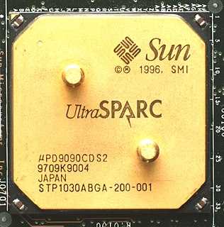
The UltraSPARC is a microprocessor developed by Sun Microsystems and fabricated by Texas Instruments, introduced in mid-1995. It is the first microprocessor from Sun to implement the 64-bit SPARC V9 instruction set architecture (ISA). Marc Tremblay was a co-microarchitect.
SPARC64 is a microprocessor developed by HAL Computer Systems and fabricated by Fujitsu. It implements the SPARC V9 instruction set architecture (ISA), the first microprocessor to do so. SPARC64 was HAL's first microprocessor and was the first in the SPARC64 brand. It operates at 101 and 118 MHz. The SPARC64 was used exclusively by Fujitsu in their systems; the first systems, the Fujitsu HALstation Model 330 and Model 350 workstations, were formally announced in September 1995 and were introduced in October 1995, two years late. It was succeeded by the SPARC64 II in 1996.

SPARCstation 5 or SS5 is a workstation introduced by Sun Microsystems in March 1994. It is based on the sun4m architecture, and is enclosed in a pizza-box chassis. Sun also offered a SPARCserver 5 without a framebuffer. A simplified, cheaper version of the SS5 was released in February 1995 as the SPARCstation 4. Sun also marketed these same machines under the "Netra" brand, without framebuffers or keyboards and preconfigured with all the requisite software to be used as web servers.

The POWER3 is a microprocessor, designed and exclusively manufactured by IBM, that implemented the 64-bit version of the PowerPC instruction set architecture (ISA), including all of the optional instructions of the ISA such as instructions present in the POWER2 version of the POWER ISA but not in the PowerPC ISA. It was introduced on 5 October 1998, debuting in the RS/6000 43P Model 260, a high-end graphics workstation. The POWER3 was originally supposed to be called the PowerPC 630 but was renamed, probably to differentiate the server-oriented POWER processors it replaced from the more consumer-oriented 32-bit PowerPCs. The POWER3 was the successor of the P2SC derivative of the POWER2 and completed IBM's long-delayed transition from POWER to PowerPC, which was originally scheduled to conclude in 1995. The POWER3 was used in IBM RS/6000 servers and workstations at 200 MHz. It competed with the Digital Equipment Corporation (DEC) Alpha 21264 and the Hewlett-Packard (HP) PA-8500.

The R10000, code-named "T5", is a RISC microprocessor implementation of the MIPS IV instruction set architecture (ISA) developed by MIPS Technologies, Inc. (MTI), then a division of Silicon Graphics, Inc. (SGI). The chief designers are Chris Rowen and Kenneth C. Yeager. The R10000 microarchitecture is known as ANDES, an abbreviation for Architecture with Non-sequential Dynamic Execution Scheduling. The R10000 largely replaces the R8000 in the high-end and the R4400 elsewhere. MTI was a fabless semiconductor company; the R10000 was fabricated by NEC and Toshiba. Previous fabricators of MIPS microprocessors such as Integrated Device Technology (IDT) and three others did not fabricate the R10000 as it was more expensive to do so than the R4000 and R4400.

The R4000 is a microprocessor developed by MIPS Computer Systems that implements the MIPS III instruction set architecture (ISA). Officially announced on 1 October 1991, it was one of the first 64-bit microprocessors and the first MIPS III implementation. In the early 1990s, when RISC microprocessors were expected to replace CISC microprocessors such as the Intel i486, the R4000 was selected to be the microprocessor of the Advanced Computing Environment (ACE), an industry standard that intended to define a common RISC platform. ACE ultimately failed for a number of reasons, but the R4000 found success in the workstation and server markets.

The R5000 is a 64-bit, little endian (mipsel) superscalar, in-order execution 2-issue design microprocessor, that implements the MIPS IV instruction set architecture (ISA) developed by Quantum Effect Design (QED) in 1996. The project was funded by MIPS Technologies, Inc (MTI), also the licensor. MTI then licensed the design to Integrated Device Technology (IDT), NEC, NKK, and Toshiba. The R5000 succeeded the QED R4600 and R4700 as their flagship high-end embedded microprocessor. IDT marketed its version of the R5000 as the 79RV5000, NEC as VR5000, NKK as the NR5000, and Toshiba as the TX5000. The R5000 was sold to PMC-Sierra when the company acquired QED. Derivatives of the R5000 are still in production today for embedded systems.
The R8000 is a microprocessor chipset developed by MIPS Technologies, Inc. (MTI), Toshiba, and Weitek. It was the first implementation of the MIPS IV instruction set architecture. The R8000 is also known as the TFP, for Tremendous Floating-Point, its name during development.

The Alpha 21064 is a microprocessor developed and fabricated by Digital Equipment Corporation that implemented the Alpha instruction set architecture (ISA). It was introduced as the DECchip 21064 before it was renamed in 1994. The 21064 is also known by its code name, EV4. It was announced in February 1992 with volume availability in September 1992. The 21064 was the first commercial implementation of the Alpha ISA, and the first microprocessor from Digital to be available commercially. It was succeeded by a derivative, the Alpha 21064A in October 1993.

The Alpha 21164, also known by its code name, EV5, is a microprocessor developed and fabricated by Digital Equipment Corporation that implemented the Alpha instruction set architecture (ISA). It was introduced in January 1995, succeeding the Alpha 21064A as Digital's flagship microprocessor. It was succeeded by the Alpha 21264 in 1998.
The Alpha 21264 is a Digital Equipment Corporation RISC microprocessor launched on 19 October 1998. The 21264 implemented the Alpha instruction set architecture (ISA).
The SPARC64 V (Zeus) is a SPARC V9 microprocessor designed by Fujitsu. The SPARC64 V was the basis for a series of successive processors designed for servers, and later, supercomputers.
The hyperSPARC, code-named "Pinnacle", is a microprocessor that implements the SPARC Version 8 instruction set architecture (ISA) developed by Ross Technology for Cypress Semiconductor.

The PA-8000 (PCX-U), code-named Onyx, is a microprocessor developed and fabricated by Hewlett-Packard (HP) that implemented the PA-RISC 2.0 instruction set architecture (ISA). It was a completely new design with no circuitry derived from previous PA-RISC microprocessors. The PA-8000 was introduced on 2 November 1995 when shipments began to members of the Precision RISC Organization (PRO). It was used exclusively by PRO members and was not sold on the merchant market. All follow-on PA-8x00 processors are based on the basic PA-8000 processor core.
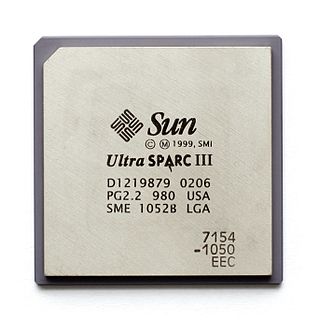
The UltraSPARC III, code-named "Cheetah", is a microprocessor that implements the SPARC V9 instruction set architecture (ISA) developed by Sun Microsystems and fabricated by Texas Instruments. It was introduced in 2001 and operates at 600 to 900 MHz. It was succeeded by the UltraSPARC IV in 2004. Gary Lauterbach was the chief architect.

The PA-7100LC is a microprocessor that implements the PA-RISC 1.1 instruction set architecture (ISA) developed by Hewlett-Packard (HP). It is also known as the PCX-L, and by its code-name, Hummingbird. It was designed as a low-cost microprocessor for low-end systems. The first systems to feature the PA-7100LC were introduced in January 1994. These systems used 60 and 80 MHz parts. A 100 MHz part debuted in June 1994. The PA-7100LC was the first PA-RISC microprocessor to implement the MAX-1 multimedia instructions, an early single instruction, multiple data (SIMD) multimedia instruction set extension that provided instructions for improving the performance of MPEG video decoding.
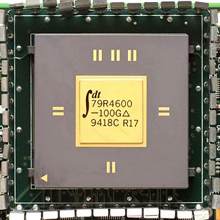
The R4600, code-named "Orion", is a microprocessor developed by Quantum Effect Design (QED) that implemented the MIPS III instruction set architecture (ISA). As QED was a design firm that did not fabricate or sell their designs, the R4600 was first licensed to Integrated Device Technology (IDT), and later to Toshiba and then NKK. These companies fabricated the microprocessor and marketed it. The R4600 was designed as a low-end workstation or high-end embedded microprocessor. Users included Silicon Graphics, Inc. (SGI) for their Indy workstation and DeskStation Technology for their Windows NT workstations. The R4600 was instrumental in making the Indy successful by providing good integer performance at a competitive price. In embedded systems, prominent users included Cisco Systems in their network routers and Canon in their printers.

The SPARCstation IPX is a workstation that was sold by Sun Microsystems, introduced July 1991. It is based on the sun4c architecture, and is enclosed in a lunchbox chassis.
Since 1985, many processors implementing some version of the MIPS architecture have been designed and used widely.

