
Wire wrap is an electronic component assembly technique that was invented to wire telephone crossbar switches, and later adapted to construct electronic circuit boards. Electronic components mounted on an insulating board are interconnected by lengths of insulated wire run between their terminals, with the connections made by wrapping several turns of uninsulated sections of the wire around a component lead or a socket pin.

A printed circuit board (PCB), also called printed wiring board (PWB), is a laminated sandwich structure of conductive and insulating layers, each with a pattern of traces, planes and other features etched from one or more sheet layers of copper laminated onto or between sheet layers of a non-conductive substrate. PCBs are used to connect or "wire" components to one another in an electronic circuit. Electrical components may be fixed to conductive pads on the outer layers, generally by soldering, which both electrically connects and mechanically fastens the components to the board. Another manufacturing process adds vias, metal-lined drilled holes that enable electrical interconnections between conductive layers, to boards with more than a single side.

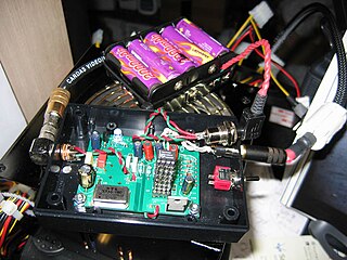
In electronics, point-to-point construction is a non-automated technique for constructing circuits which was widely used before the use of printed circuit boards (PCBs) and automated assembly gradually became widespread following their introduction in the 1950s. Circuits using thermionic valves were relatively large, relatively simple, and used large sockets, all of which made the PCB less obviously advantageous than with later complex semiconductor circuits. Point-to-point construction is still widespread in power electronics, where components are bulky and serviceability is a consideration, and to construct prototype equipment with few or heavy electronic components. A common practice, especially in older point-to-point construction, is to use the leads of components such as resistors and capacitors to bridge as much of the distance between connections as possible, reducing the need to add additional wire between the components.

A breadboard, solderless breadboard, or protoboard is a construction base used to build semi-permanent prototypes of electronic circuits. Unlike a perfboard or stripboard, breadboards do not require soldering or destruction of tracks and are hence reusable. For this reason, breadboards are also popular with students and in technological education.

Surface-mount technology (SMT), originally called planar mounting, is a method in which the electrical components are mounted directly onto the surface of a printed circuit board (PCB). An electrical component mounted in this manner is referred to as a surface-mount device (SMD). In industry, this approach has largely replaced the through-hole technology construction method of fitting components, in large part because SMT allows for increased manufacturing automation which reduces cost and improves quality. It also allows for more components to fit on a given area of substrate. Both technologies can be used on the same board, with the through-hole technology often used for components not suitable for surface mounting such as large transformers and heat-sinked power semiconductors.

Stripboard is the generic name for a widely used type of electronics prototyping material for circuit boards characterized by a pre-formed 0.1 inches (2.54 mm) regular (rectangular) grid of holes, with wide parallel strips of copper cladding running in one direction all the way along one side of an insulating bonded paper board. It is commonly also known by the name of the original product Veroboard, which is a trademark, in the UK, of British company Vero Technologies Ltd and Canadian company Pixel Print Ltd. It was originated and developed in the early 1960s by the Electronics Department of Vero Precision Engineering Ltd (VPE). It was introduced as a general-purpose material for use in constructing electronic circuits - differing from purpose-designed printed circuit boards (PCBs) in that a variety of electronics circuits may be constructed using a standard wiring board.
Place and route is a stage in the design of printed circuit boards, integrated circuits, and field-programmable gate arrays. As implied by the name, it is composed of two steps, placement and routing. The first step, placement, involves deciding where to place all electronic components, circuitry, and logic elements in a generally limited amount of space. This is followed by routing, which decides the exact design of all the wires needed to connect the placed components. This step must implement all the desired connections while following the rules and limitations of the manufacturing process.

In electronics, through-hole technology is a manufacturing scheme in which leads on the components are inserted through holes drilled in printed circuit boards (PCB) and soldered to pads on the opposite side, either by manual assembly or by the use of automated insertion mount machines.
DIY Audio, do it yourself audio. Rather than buying a piece of possibly expensive audio equipment, such as a high-end audio amplifier or speaker, the person practicing DIY Audio will make it themselves. Alternatively, a DIYer may take an existing manufactured item of vintage era and update or modify it. The benefits of doing so include the satisfaction of creating something enjoyable, the possibility that the equipment made or updated is of higher quality than commercially available products and the pleasure of creating a custom-made device for which no exact equivalent is marketed. Other motivations for DIY audio can include getting audio components at a lower cost, the entertainment of using the item, and being able to ensure quality of workmanship.

A via is an electrical connection between two or more metal layers of a printed circuit boards (PCB) or integrated circuit. Essentially a via is a small drilled hole that goes through two or more adjacent layers; the hole is plated with metal that forms an electrical connection through the insulating layers.

An electronic kit is a package of electrical components used to build an electronic device. Generally, kits are composed of electronic components, a circuit diagram (schematic), assembly instructions, and often a printed circuit board (PCB) or another type of prototyping board.

Flat no-leads packages such as quad-flat no-leads (QFN) and dual-flat no-leads (DFN) physically and electrically connect integrated circuits to printed circuit boards. Flat no-leads, also known as micro leadframe (MLF) and SON, is a surface-mount technology, one of several package technologies that connect ICs to the surfaces of PCBs without through-holes. Flat no-lead is a near chip scale plastic encapsulated package made with a planar copper lead frame substrate. Perimeter lands on the package bottom provide electrical connections to the PCB. Flat no-lead packages usually, but not always, include an exposed thermally conductive pad to improve heat transfer out of the IC. Heat transfer can be further facilitated by metal vias in the thermal pad. The QFN package is similar to the quad-flat package (QFP), and a ball grid array (BGA).

Perfboard is a material for prototyping electronic circuits. It is a thin, rigid sheet with holes pre-drilled at standard intervals across a grid, usually a square grid of 0.1 inches (2.54 mm) spacing. These holes are ringed by round or square copper pads, though bare boards are also available. Inexpensive perfboard may have pads on only one side of the board, while better quality perfboard can have pads on both sides. Since each pad is electrically isolated, the builder makes all connections with either wire wrap or miniature point to point wiring techniques. Discrete components are soldered to the prototype board such as resistors, capacitors, and integrated circuits. The substrate is typically made of paper laminated with phenolic resin or a fiberglass-reinforced epoxy laminate (FR-4).

Automated optical inspection (AOI) is an automated visual inspection of printed circuit board (PCB) manufacture where a camera autonomously scans the device under test for both catastrophic failure and quality defects. It is commonly used in the manufacturing process because it is a non-contact test method. It is implemented at many stages through the manufacturing process including bare board inspection, solder paste inspection (SPI), pre-reflow and post-re-flow as well as other stages.
A semiconductor package is a metal, plastic, glass, or ceramic casing containing one or more discrete semiconductor devices or integrated circuits. Individual components are fabricated on semiconductor wafers before being diced into die, tested, and packaged. The package provides a means for connecting it to the external environment, such as printed circuit board, via leads such as lands, balls, or pins; and protection against threats such as mechanical impact, chemical contamination, and light exposure. Additionally, it helps dissipate heat produced by the device, with or without the aid of a heat spreader. There are thousands of package types in use. Some are defined by international, national, or industry standards, while others are particular to an individual manufacturer.
The Occam process is a solder-free, Restriction of Hazardous Substances Directive (RoHS)-compliant method for use in circuit board manufacturing developed by Verdant Electronics. It combines the usual two steps of constructing printed circuit boards (PCBs) followed by the population process of placing various leaded and non-leaded electronic components into one process. The name "Occam" comes from a quotation by William of Ockham.

DipTrace is a proprietary software suite for electronic design automation (EDA) used for electronic schematic capture and printed circuit board layouts. DipTrace has four applications: schematic editor, PCB editor with built-in shape-based autorouter and 3D preview, component editor, and pattern editor.
In electronics, a cross section, cross-section, or microsection, is a prepared electronics sample that allows analysis at a plane that cuts through the sample. It is a destructive technique requiring that a portion of the sample be cut or ground away to expose the internal plane for analysis. They are commonly prepared for research, manufacturing quality assurance, supplier conformity, and failure analysis. Printed wiring boards (PWBs) and electronic components and their solder joints are common cross sectioned samples. The features of interest to be analyzed in cross section can be nanometer-scale metal and dielectric layers in semiconductors up to macroscopic features such as the amount of solder that has filled into a large, 0.125in (3.18mm) diameter plated-through hole.

In electronics, prototyping means building an actual circuit to a theoretical design to verify that it works, and to provide a physical platform for debugging it if it does not. The prototype is often constructed using techniques such as wire wrapping or using a breadboard, stripboard or perfboard, with the result being a circuit that is electrically identical to the design but not physically identical to the final product.

Printed circuit board manufacturing is the process of manufacturing bare printed circuit boards (PCBs) and then populating them with electronic components. It involves the full assembly of a board into a functional circuit board.


