Carbon nanobud

Last updated

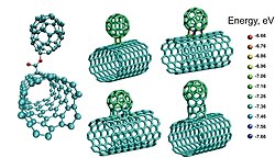
Computer models of several stable nanobud structures NanobudComputations70%25.jpg
Computer models of several stable nanobud structures
In situ observation of a carbon nanobud by transmission electron microscopy [1]
Capture of an additional fullerene molecule by a nanobud [1]
Generation of fullerene molecules (carbon peapod) inside a nanobud [1]

In nanotechnology, a carbon nanobud is a material that combines carbon nanotubes and spheroidal fullerenes, both allotropes of carbon, forming "buds" attached to the tubes. Carbon nanobuds were discovered and synthesized in 2006. [2]

Contents

In this material, fullerenes are bonded with covalent bonds to the outer sidewalls of the underlying nanotube. Consequently, nanobuds exhibit properties of both carbon nanotubes and fullerenes. For instance, the mechanical property and the electrical conductivity of the nanobuds are similar to those of corresponding carbon nanotubes. However, because of the higher reactivity of the attached fullerene molecules, the hybrid material can be further functionalized through known fullerene chemistry. Additionally, the attached fullerene molecules can be used as molecular anchors to prevent the slipping of the nanotubes in various composite materials, thus modifying the mechanical properties of the composite. [3] [4]

Owing to a large number of highly curved fullerene surfaces acting as electron emission sites on conductive carbon nanotubes, nanobuds possess advantageous field electron emission characteristics. Randomly oriented nanobuds have already been demonstrated to have lesser work function for field electron emission. Reported test measurements show (macroscopic) field thresholds of about 0.65 V/μm (non-functionalized single-walled carbon nanotubes have a macroscopic field threshold for field electron emission ~2 V/μm) and a much higher current density as compared with that of the corresponding pure single-walled carbon nanotubes. [3] The electron transport properties of certain nanobud classes have been analyzed theoretically. [5] The study shows that electrons indeed migrate to the neck and bud region of the nanobud system.

Canatu Oy, a Finnish company, claims the intellectual property rights for nanobud material, its synthesis processes, and several applications. [6]

Properties

Carbon nanobuds (CNBs) have some of the properties of carbon nanotubes, such as one-dimensional electrical conductivity, flexibility and manufacturing adaptability, as well as some of the chemical properties of fullerenes. Examples of these properties include ability to engage in cycloaddition reactions and can easily form the chemical bonds capable of attaching to other molecules with complex structures. CNBs have a much higher chemical activity than single-walled carbon nanotubes (SWCNTs). [7]

Electrical Properties

This new structure has been shown to have electronic properties that differ from those of fullerenes and carbon nanotubes (CNTs). CNBs exhibit lower field thresholds, higher current densities, and electric field emissions than SWCNTs. [8] The chemical bonds between the nanotube's wall and the fullerenes on the surface can lead to charge transfer between the surfaces. [8] The presence of fullerenes in CNBs leads to smaller bundle formation and higher chemical reactivity. [8] CNBs can engage in cycloaddition reactions and easily form chemical bonds capable of attaching molecules with complex structures. It can be explained by the greater availability of CNB surface to the reactants, the presence of π-conjugated structure and 5-atom rings with excess pirimidization energy. [9] Formation energy indicated that the preparation of CNBs is endothermic, meaning that it is not favorable to create. [10]

All CNBs are conducting, regardless of whether the single-walled CNT is a metallic or semiconducting base. The band gap of carbon nanobuds is not constant. It can change through the size of the fullerene group. [7] The attachment of C60 added to the armchair orientation of the SWCNT opens up the band gap. On the other hand, adding it to a semiconducting SWCNT could introduce impurity states to the band gap, which would reduce the band gap. The band gap of CNBs can also be modified by changing the density of the carbons of the C60 attached to the sidewall of the SWCNT. [11]

Magnetic Properties

Geometrical factors are integral to studying the magnetic properties of nanobuds. Two structures of CNBs are ferromagnetic in their ground state, and two are nonmagnetic. [12] The attached C60 molecule on the surface of the CNTs gives more space between the nanotubes-and adhesion between the single-walled CNTS can be weakened to prevent the formation of tight bundles of CNTs. [7] Carbon nanobuds can be used as molecular support to prevent the matrix from slipping into composite materials and increasing their mechanical strength. [8]

Structural Properties

The stability of CNBs are depends on the type of carbon-carbon bond that is dissociated in the cycloaddition reaction. It has been shown that carbon atoms of the SWCNT near the fullerene C60 molecule were pulled outward from the original wall surface due to the covalent bonding with cycloaddition reaction between the fullerene and nanotube; in addition, their bonding was transformed from sp2 to sp3 hybridization. [8] An analysis using Raman scattering spectroscopy shows that the CNB sample had stronger chemical modification compared to CNTs. It indicates that there is a carbon sp3 hybridization, that occurs after the chemical addition creation of CNBs. [7]

Synthesis

The single wall carbon nanotubes can react with fullerenes in the presence of water vapor or carbon dioxide. It produces a covalently linked material that looks similar to buds on a tree branch, hence the name "Nanobud". [9]

The nanobuds form in abundance at 45ppm of water vapour and higher. However, above 365 ppm, the reaction will give a higher number of inactive catalyst particles in lieu of the NanoBud. [9]

Characterization

Multiple methods are involved in discovering the fullerenes on the single-wall carbon nanotube surfaces, each giving its own contribution to what is currently known about nanobuds. A few of these methods are ultraviolet-visible spectroscopy (UV-Vis), transmission electron microscopy (TEM), and scanning tunneling microscopy (STM).

Calculations were carried out to look even further into the functionality of CNBs and understand how the single-wall carbon nanotubes interact with the fullerenes to produce the nanobuds. The calculations came from the atomistic density functional theory (quantum mechanical modelling method) and gave quite a bit of information about the bonding that is taking place. They told the scientists that there exist two possibilities for the interaction. One of the possibilities is that the fullerenes can be bonded with covalent bonds to the single wall carbon nanotubes directly. The other possibility is that the fullerenes are forming hybrid structures. [9]

Regardless of how they get attached to the single wall nanotubes, studies have shown that the fullerenes are stationary and do not seem to want to move from the interaction with the nanotubes, concluding that they have stronger bond. This study was done using transmission electron microscopy.

Another study was done to see how washing the nanobuds in different solvents, such as toluene, decalin, and hexane, would affect the fullerenes and their interaction with the nanotubes. Among the solvents that were tested, none of them resulted in fullerenes being dissolved in the solvent. It continues to defend the discovery that the bond between the two is significantly strong. It was discovered in another study that each of the nanobud samples contained oxygen. [3]

Applications

The research, development, and manufacture of flexible and transparent electronics relies on novel materials, or materials which are mechanically flexible, lightweight and relatively low cost. These materials must also be conductive and optically transparent. Due to their close relation to the carbon nanotube family, carbon nanobuds contain all of those traits, as well as more due to their inclusion of fullerene.

Carbon nanobuds have properties that are often associated with cold electron field emitters. [13] Such materials emits electrons at room temperature under a high applied electric field, a property that is very important in flat-panel displays and electron microscopes. [13] Carbon nanobuds can be more effective than flat surfaces to emit electrons due to the many curved surfaces of both the fullerene and the carbon nanotube that make up the carbon nanobud.

As a result of the curvature of the fullerenes and the nanotubes, almost any surface could potentially be transformed into a surface with touch sensing ability. Canatu, a company which specializes in electronic carbon nanobud products, claims that the films that result from the synthesis of the nanobuds are very rugged and flexible. They also claim that the nanobuds allow for easy application to flexible and curved surfaces. nanobuds are able to maintain their electronic capabilities while being bent up to 200 percent. This property is a result of the rounded surfaces, which allow the nanobuds to slide past each other without damaging the electronic structure of the material. [14] Typically, touch screen surfaces are made by placing a sheet of indium tin oxide, also a transparent film, over a display screen. However, indium tin oxide sheets are very brittle like glass and can only be applied to relatively flat surfaces in order to maintain the integrity of the structure. [14]

As a result of their close lineage with carbon nanotubes, nanobuds have a tunable electrical conductivity. [15] Since the electrical properties of the Nanobuds can be individually tuned (provided that single wall nanotubes with distinct regions of different electrical properties are a part of the Nanobud), according to Esko Kauppinen and his team, it is entirely possible that nanobuds may at some point be used in applications such as memory storage devices and quantum dots. The Kauppinen team argues that the conductivity of the crystalline carbon structure allow for this application. In fact, the small size of carbon nanotubes and carbon Nanobuds, in theory, allow for a very high density of energy storage. [16] The most common memory technology that is associated with carbon nanobuds is nano-random-access memory (NRAM), or nano-RAM. This technology is a type of nonvolatile random access memory, but it is based on the position of carbon nanotubes, or in this case, carbon nanobuds on a chip like substrate. [16] It is designated as NRAM by its developing company Nantero. When compared to other forms of nonvolatile random access memory, NRAM has several advantages.[ clarification needed ] NRAM is believed to be within a variety of new memory systems, a variety of which many people believe to be universal. Nantero claims that Nano-RAM (NRAM) could eventually replace almost all memory systems from flash to DRAM to SRAM.

See also

Related Research Articles

<span class="mw-page-title-main">Carbon nanotube</span> Allotropes of carbon with a cylindrical nanostructure

A carbon nanotube (CNT) is a tube made of carbon with diameters typically measured in nanometers.

Fullerene Allotrope of carbon

A fullerene is an allotrope of carbon whose molecule consists of carbon atoms connected by single and double bonds so as to form a closed or partially closed mesh, with fused rings of five to seven atoms. The molecule may be a hollow sphere, ellipsoid, tube, or many other shapes and sizes. Graphene, which is a flat mesh of regular hexagonal rings, can be seen as an extreme member of the family.

Hybrid solar cells combine advantages of both organic and inorganic semiconductors. Hybrid photovoltaics have organic materials that consist of conjugated polymers that absorb light as the donor and transport holes. Inorganic materials in hybrid cells are used as the acceptor and electron transporter in the structure. The hybrid photovoltaic devices have a potential for not only low-cost by roll-to-roll processing but also for scalable solar power conversion.

Potential applications of carbon nanotubes

Carbon nanotubes (CNTs) are cylinders of one or more layers of graphene (lattice). Diameters of single-walled carbon nanotubes (SWNTs) and multi-walled carbon nanotubes (MWNTs) are typically 0.8 to 2 nm and 5 to 20 nm, respectively, although MWNT diameters can exceed 100 nm. CNT lengths range from less than 100 nm to 0.5 m.

Selective chemistry of single-walled nanotubes is a field in Carbon nanotube chemistry devoted specifically to the study of functionalization of single-walled carbon nanotubes.

Organic photovoltaic devices (OPVs) are fabricated from thin films of organic semiconductors, such as polymers and small-molecule compounds, and are typically on the order of 100 nm thick. Because polymer based OPVs can be made using a coating process such as spin coating or inkjet printing, they are an attractive option for inexpensively covering large areas as well as flexible plastic surfaces. A promising low cost alternative to conventional solar cells made of crystalline silicon, there is a large amount of research being dedicated throughout industry and academia towards developing OPVs and increasing their power conversion efficiency.

Optical properties of carbon nanotubes Optical properties of the material

The optical properties of carbon nanotubes are highly relevant for materials science. The way those materials interact with electromagnetic radiation is unique in many respects, as evidenced by their peculiar absorption, photoluminescence (fluorescence), and Raman spectra.

Carbon nanotubes (CNTs) are very prevalent in today's world of medical research and are being highly researched in the fields of efficient drug delivery and biosensing methods for disease treatment and health monitoring. Carbon nanotube technology has shown to have the potential to alter drug delivery and biosensing methods for the better, and thus, carbon nanotubes have recently garnered interest in the field of medicine.

In polymer chemistry, in situ polymerization is a preparation method that occurs "in the polymerization mixture" and is used to develop polymer nanocomposites from nanoparticles. There are numerous unstable oligomers (molecules) which must be synthesized in situ for use in various processes. The in situ polymerization process consists of an initiation step followed by a series of polymerization steps, which results in the formation of a hybrid between polymer molecules and nanoparticles. Nanoparticles are initially spread out in a liquid monomer or a precursor of relatively low molecular weight. Upon the formation of a homogeneous mixture, initiation of the polymerization reaction is carried out by addition of an adequate initiator, which is exposed to a source of heat, radiation, etc. After the polymerization mechanism is completed, a nanocomposite is produced, which consists of polymer molecules bound to nanoparticles.

Self-assembling peptides are a category of peptides which undergo spontaneous assembling into ordered nanostructures. Originally described in 1993, these designer peptides have attracted interest in the field of nanotechnology for their potential for application in areas such as biomedical nanotechnology, tissue cell culturing, molecular electronics, and more.

Carbon nanotube chemistry

Carbon nanotube chemistry involves chemical reactions, which are used to modify the properties of carbon nanotubes (CNTs). CNTs can be functionalized to attain desired properties that can be used in a wide variety of applications. The two main methods of CNT functionalization are covalent and non-covalent modifications.

Single-walled carbon nanohorn

Single-walled carbon nanohorn is the name given by Sumio Iijima and colleagues in 1999 to horn-shaped sheath aggregate of graphene sheets. Very similar structures had been observed in 1994 by Peter J.F. Harris, Edman Tsang, John Claridge and Malcolm Green. Ever since the discovery of the fullerene, the family of carbon nanostructures has been steadily expanded. Included in this family are single-walled and multi-walled carbon nanotubes, carbon onions and cones and, most recently, SWNHs. These SWNHs with about 40–50 nm in tubule length and about 2–3 nm in diameter are derived from SWNTs and ended by a five-pentagon conical cap with a cone opening angle of ~20o. Moreover, thousands of SWNHs associate with each other to form the ‘dahlia-like' and ‘bud-like’ structured aggregates which have an average diameter of about 80–100 nm. The former consists of tubules and graphene sheets protruding from its surface like petals of a dahlia, while the latter is composed of tubules developing inside the particle itself. Their unique structures with high surface area and microporosity make SWNHs become a promising material for gas adsorption, biosensing, drug delivery, gas storage and catalyst support for fuel cell. Single-walled carbon nanohorns are an example of the family of carbon nanocones.

Carbon nanotube supported catalyst

Carbon nanotube supported catalyst is a novel supported catalyst, using carbon nanotubes as the support instead of the conventional alumina or silicon support. The exceptional physical properties of carbon nanotubes (CNTs) such as large specific surface areas, excellent electron conductivity incorporated with the good chemical inertness, and relatively high oxidation stability makes it a promising support material for heterogeneous catalysis.

Carbon nanothread

A carbon nanothread is a sp3-bonded, one-dimensional carbon crystalline nanomaterial. The tetrahedral sp3-bonding of its carbon is similar to that of diamond. Nanothreads are only a few atoms across, more than 20,000 times thinner than a human hair. They consist of a stiff, strong carbon core surrounded by hydrogen atoms. Carbon nanotubes, although also one-dimensional nanomaterials, in contrast have sp2-carbon bonding as is found in graphite. The smallest carbon nanothread has a diameter of only 0.2 nanometer, much smaller than the diameter of a single-wall carbon nanotube.

Carbon peapod Hybrid nanomaterial

Carbon peapod is a hybrid nanomaterial consisting of spheroidal fullerenes encapsulated within a carbon nanotube. It is named due to their resemblance to the seedpod of the pea plant. Since the properties of carbon peapods differ from those of nanotubes and fullerenes, the carbon peapod can be recognized as a new type of a self-assembled graphitic structure. Possible applications of nano-peapods include nanoscale lasers, single electron transistors, spin-qubit arrays for quantum computing, nanopipettes, and data storage devices thanks to the memory effects and superconductivity of nano-peapods.

Water shortages have become an increasingly pressing concern recently and with recent predictions of a high probability of the current drought turning into a megadrought occurring in the western United States, technologies involving water treatment and processing need to improve. Carbon nanotubes (CNT) have been the subject of extensive studies because they demonstrate a range of unique properties that existing technologies lack. For example, carbon nanotube membranes can demonstrate higher water flux with lower energy than current membranes. These membranes can also filter out particles that are too small for conventional systems which can lead to better water purification techniques and less waste. The largest obstacle facing CNT is processing as it is difficult to produce them in the large quantities that most of these technologies will require.

Toxicology of carbon nanomaterials Overview of toxicology of carbon nanomaterials

There has been much research on the nanotoxicology of fullerenes and carbon nanotubes.

Vertically aligned carbon nanotube arrays (VANTAs) are a unique microstructure consisting of carbon nanotubes oriented with their longitudinal axis perpendicular to a substrate surface. These VANTAs effectively preserve and often accentuate the unique anisotropic properties of individual carbon nanotubes and possess a morphology that may be precisely controlled. VANTAs are consequently widely useful in a range of current and potential device applications.

There are many water purifiers available in the market which use different techniques like boiling, filtration, distillation, chlorination, sedimentation and oxidation. Currently nanotechnology plays a vital role in water purification techniques. Nanotechnology is the process of manipulating atoms on a nanoscale. In nanotechnology, nano membranes are used with the purpose of softening the water and removal of contaminants such as physical, biological and chemical contaminants. There are variety of techniques in nanotechnology which uses nano particles for providing safe drinking water with a high level of effectiveness. Some techniques have become commercialized.

Andrew R. Barron is a British chemist, academic, and entrepreneur. He is the Sêr Cymru Chair of Low Carbon Energy and Environment at Swansea University, and the Charles W. Duncan Jr.-Welch Foundation Chair in Chemistry at Rice University. He is the founder and director of Energy Safety Research Institute (ESRI) at Swansea University, which consolidates the energy research at the University with a focus on environmental impact and future security. At Rice University, he leads a Research Group and has served as Associate Dean for Industry Interactions and Technology Transfer.

References

  1. 1 2 3 Gorantla, Sandeep; Börrnert, Felix; Bachmatiuk, Alicja; Dimitrakopoulou, Maria; Schönfelder, Ronny; Schäffel, Franziska; Thomas, Jürgen; Gemming, Thomas; Borowiak-Palen, Ewa; Warner, Jamie H.; Yakobson, Boris I.; Eckert, Jürgen; Büchner, Bernd; Rümmeli, Mark H. (2010). "In situ observations of fullerene fusion and ejection in carbon nanotubes". Nanoscale. 2 (10): 2077. Bibcode:2010Nanos...2.2077G. doi:10.1039/C0NR00426J. PMID   20714658.
  2. Nasibulin, Albert G.; Pikhitsa, Peter V.; Jiang, Hua; Brown, David P.; Krasheninnikov, Arkady V.; Anisimov, Anton S.; Queipo, Paula; Moisala, Anna; Gonzalez, David; Lientschnig, Günther; Hassanien, Abdou (March 2007). "A novel hybrid carbon material". Nature Nanotechnology. 2 (3): 156–161. doi:10.1038/nnano.2007.37. ISSN   1748-3395.
  3. 1 2 3 Nasibulin, Albert G.; et al. (2007). "A novel hybrid carbon material" (PDF). Nature Nanotechnology . 2 (3): 156–161. Bibcode:2007NatNa...2..156N. doi:10.1038/nnano.2007.37. PMID   18654245. Archived from the original (PDF) on 26 February 2012. Retrieved 31 August 2009.
  4. Nasibulin, Albert G.; et al. (2007). "Investigations of NanoBud formation" (PDF). Chemical Physics Letters. 446: 109–114. Bibcode:2007CPL...446..109N. doi:10.1016/j.cplett.2007.08.050. Archived from the original (PDF) on 20 July 2011. Retrieved 31 August 2009.
  5. Fürst, Joachim A.; et al. (2009). "Electronic transport properties of fullerene functionalized carbon nanotubes: Ab initio and tight-binding calculations" (PDF). Physical Review B . 80 (3): 115117. doi:10.1103/PhysRevB.80.035427.
  6. "European Patent Office: search CANATU" . Retrieved 3 June 2010.
  7. 1 2 3 4 Albert G. Nasibulin Ilya V. Anoshkin, Prasantha R. Mudimela, Janne Raula, Vladimir Ermolov, Esko I. Kauppinen, "Selective Chemical Functionalization of Carbon Nanobuds," Carbon 50, no. 11 (2012).
  8. 1 2 3 4 5 Ahangari, M. Ghorbanzadeh; Ganji, M.D.; Montazar, F. (2015). "Mechanical and Electronic Properties of Carbon Nanobuds: First-Principles Study". Solid State Communications. 203: 58–62.
  9. 1 2 3 4 Anisimov, Anton. "Aerosol Synthesis of Carbon Nanotubes and Nanobuds.". (2010).
  10. Seif, A.; Zahedi, E.; Ahmadi, T. S. (2011). "A Dft Study of Carbon Nanobuds". The European Physical Journal B. 82 (2): 147–52.
  11. Xiaojun Wu and Xiao Cheng Zeng, "First-Principles Study of a Carbon Nanobud," ACS Nano 2, no. 7 (2008)
  12. Min Wang and Chang Ming Li, "Magnetic Properties of All-Carbon Graphene-Fullerene Nanobuds," Physical Chemistry Chemical Physics 13, no. 13 (2011).
  13. 1 2 Clarke, Peter (21 November 2014). "Carbon 'nanobuds' enable transparent touch sensors on 3D surfaces". Eenewsanalog.com.
  14. 1 2 Bullis, Kevin (11 December 2014). "Startup Tests Nanobud Touch Sensors". MIT Technology Review.
  15. Mgrdichian, Laura (30 March 2007). "New Nanomaterial, NanoBuds, Combines Fullerenes and ..."
  16. 1 2 "Electronics". Nanotechmag.com.