Related Research Articles

A laser diode is a semiconductor device similar to a light-emitting diode in which a diode pumped directly with electrical current can create lasing conditions at the diode's junction.

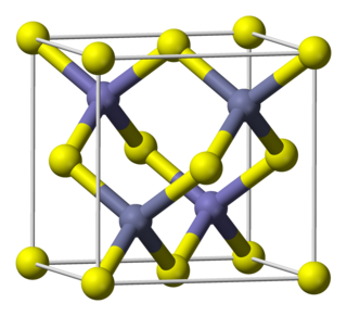
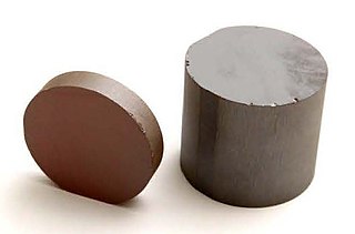
Gallium arsenide (GaAs) is a III-V direct band gap semiconductor with a zinc blende crystal structure.
Indium phosphide (InP) is a binary semiconductor composed of indium and phosphorus. It has a face-centered cubic ("zincblende") crystal structure, identical to that of GaAs and most of the III-V semiconductors.
The heterojunction bipolar transistor (HBT) is a type of bipolar junction transistor (BJT) which uses differing semiconductor materials for the emitter and base regions, creating a heterojunction. The HBT improves on the BJT in that it can handle signals of very high frequencies, up to several hundred GHz. It is commonly used in modern ultrafast circuits, mostly radio frequency (RF) systems, and in applications requiring a high power efficiency, such as RF power amplifiers in cellular phones. The idea of employing a heterojunction is as old as the conventional BJT, dating back to a patent from 1951. Detailed theory of heterojunction bipolar transistor was developed by Herbert Kroemer in 1957.
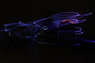
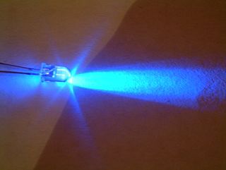
A blue laser is a laser that emits electromagnetic radiation with a wavelength between 360 and 480 nanometers, which the human eye sees as blue or violet.
Indium gallium phosphide (InGaP), also called gallium indium phosphide (GaInP), is a semiconductor composed of indium, gallium and phosphorus. It is used in high-power and high-frequency electronics because of its superior electron velocity with respect to the more common semiconductors silicon and gallium arsenide.
Indium gallium nitride is a semiconductor material made of a mix of gallium nitride (GaN) and indium nitride (InN). It is a ternary group III/group V direct bandgap semiconductor. Its bandgap can be tuned by varying the amount of indium in the alloy. InxGa1−xN has a direct bandgap span from the infrared for InN to the ultraviolet of GaN. The ratio of In/Ga is usually between 0.02/0.98 and 0.3/0.7.
Indium arsenide, InAs, or indium monoarsenide, is a narrow-bandgap semiconductor composed of indium and arsenic. It has the appearance of grey cubic crystals with a melting point of 942 °C.
Gallium phosphide (GaP), a phosphide of gallium, is a compound semiconductor material with an indirect band gap of 2.24 eV at room temperature. Impure polycrystalline material has the appearance of pale orange or grayish pieces. Undoped single crystals are orange, but strongly doped wafers appear darker due to free-carrier absorption. It is odorless and insoluble in water.
Aluminium gallium indium phosphide is a semiconductor material that provides a platform for the development of novel multi-junction photovoltaics and optoelectronic devices, as it spans a direct bandgap from deep ultraviolet to infrared.
Aluminium gallium phosphide, (Al,Ga)P, a phosphide of aluminium and gallium, is a semiconductor material. It is an alloy of aluminium phosphide and gallium phosphide. It is used to manufacture light-emitting diodes emitting green light.
Milton Feng co-created the first transistor laser, working with Nick Holonyak in 2004. The paper discussing their work was voted in 2006 as one of the five most important papers published by the American Institute of Physics since its founding 75 years ago. In addition to the invention of transistor laser, he is also well known for inventions of other "major breakthrough" devices, including the world's fastest transistor and light-emitting transistor (LET). As of May, 2009 he is a professor at the University of Illinois at Urbana–Champaign and holds the Nick Holonyak Jr. Endowed Chair Professorship.
A quantum well laser is a laser diode in which the active region of the device is so narrow that quantum confinement occurs. Laser diodes are formed in compound semiconductor materials that are able to emit light efficiently. The wavelength of the light emitted by a quantum well laser is determined by the width of the active region rather than just the bandgap of the materials from which it is constructed. This means that much shorter wavelengths can be obtained from quantum well lasers than from conventional laser diodes using a particular semiconductor material. The efficiency of a quantum well laser is also greater than a conventional laser diode due to the stepwise form of its density of states function.
Gallium indium arsenide antimonide phosphide is a semiconductor material.
IQE plc is a British semiconductor company founded 1988 in Cardiff, Wales, which manufactures advanced epitaxial wafers for a wide range of technology applications for wireless, optoelectronic, electronic and solar devices. IQE specialises in advanced silicon and compound semiconductor materials based on gallium arsenide (GaAs), indium phosphide (InP), gallium nitride (GaN) and silicon. The company is the largest independent outsource producer of epiwafers manufactured by metalorganic vapour phase epitaxy (MOCVD), molecular beam epitaxy (MBE) and chemical vapor deposition (CVD).
Indium arsenide antimonide phosphide is a semiconductor material.
Indium gallium arsenide phosphide is a quaternary compound semiconductor material, an alloy of gallium arsenide, gallium phosphide, indium arsenide, or indium phosphide. This compound has applications in photonic devices, due to the ability to tailor its band gap via changes in the alloy mole ratios, x and y.
A light-emitting transistor or LET is a form of transistor that emits light. Higher efficiency than light-emitting diode (LED) is possible.
Rubin Braunstein (1922–2018) was an American physicist and educator. In 1955 he published the first measurements of light emission by semiconductor diodes made from crystals of gallium arsenide (GaAs), gallium antimonide (GaSb), and indium phosphide (InP). GaAs, GaSb, and InP are examples of III-V semiconductors. The III-V semiconductors absorb and emit light much more strongly than silicon, which is the best-known semiconductor. Braunstein's devices are the forerunners of contemporary LED lighting and semiconductor lasers, which typically employ III-V semiconductors. The 2000 and 2014 Nobel Prizes in Physics were awarded for further advances in closely related fields.
References
- ↑ Tadashige Sato and Megumi Imai (2002). "Characteristics of Nitrogen-Doped GaAsP Light-Emitting Diodes". Japanese Journal of Applied Physics. 41: 5995–5998. doi:10.1143/JJAP.41.5995. S2CID 119751060.
| | This condensed matter physics-related article is a stub. You can help Wikipedia by expanding it. |